AD7834/AD7835
AD7835 PIN DESCRIPTION
Pin Mnemonic
Description
VCC
Logic Power Supply; +5 V ± 5%.
VSS
Negative Analog Power Supply; –15 V ± 5%.
Positive Analog Power Supply; +15 V ± 5%.
Digital Ground.
VDD
DGND
AGND
Analog Ground.
VREF(+)A, VREF(–)A
VREF(+)B, VREF(–)B
Reference Inputs for DACs 1 and 2. These reference voltages are referred to AGND.
Reference Inputs for DACs 3 and 4. These reference voltages are referred to AGND.
DAC Outputs.
VOUT1 . . . VOUT
CS
4
Level-Triggered Chip Select Input (active low). The device is selected when this input is low.
DB0 . . . DB13
Parallel Data Inputs. The AD7835 can accept a straight 14-bit parallel word on DB0 to DB13, where
DB13 is the MSB and the BYSHF input is hardwired to a logic high. Alternatively for byte loading, the
bottom 8 data inputs, DB0–DB7, are used for data loading while the top 6 data inputs, DB8 to DB13,
should be hardwired to a logic low. The BYSHF control input selects whether 8 LSBs or 6 MSBs of data
are being loaded into the device.
BYSHF
Byte Shift Input. When low, it shifts the data on DB0–DB7 into the DB8–DB13 half of the input register.
A0, A1, A2
Address inputs. A0 and A1 are decoded to select one of the four input latches for a data transfer. A2 is
used to select all four DACs simultaneously.
LDAC
Load DAC Input (level sensitive). This input signal in conjunction with the WR and CS input signals, de-
termines how the analog outputs are updated. If LDAC is maintained high while new data is being loaded
into the device’s input registers, no change occurs on the analog outputs. Subsequently, when LDAC is
brought low, the contents of all four input registers are transferred into their respective DAC latches, up-
dating the analog outputs simultaneously.
Alternatively, if LDAC is brought low while new data is being entered, then the addressed DAC latch
(and corresponding analog output) is updated immediately on the rising edge of WR.
CLR
Asynchronous Clear Input (level sensitive, active low). When this input is brought low, all analog outputs
are switched to the externally set potentials on the DSG pins (VOUT1 and VOUT2 follow DSGA while
V
OUT3 and VOUT4 follow DSGB). When CLR is brought high, the signal outputs remain at the DSG po-
tentials until LDAC is brought low. When LDAC is brought low, the analog outputs are switched back to
reflect their individual DAC output levels. As long as CLR remains low, the LDAC signals are ignored
and the signal outputs remain switched to the potential on the DSG pins.
WR
Level-Triggered Write Input (active low). When active it is used in conjunction with CS to write data over
the input data bus.
DSGA
DSGB
Device Sense Ground A Input. Used in conjunction with the CLR input for power-on protection of the
DACs. When CLR is low, DAC outputs VOUT1 and VOUT2 are forced to the potential on the DSGA pin.
Device Sense Ground B Input. Used in conjunction with the CLR input for power-on protection of the
DACs. When CLR is low, DAC outputs VOUT3 and VOUT4 are forced to the potential on the DSGB pin.
–6–
REV. A


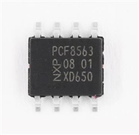
 pcf8563芯片功能说明、参数分析、引脚说明

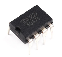
 TDA2822资料手册:引脚说明、参数分析

 TJA1050资料数据分析、引脚说明、应用示例介绍

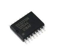
 DS3231时钟芯片:参数分析、引脚说明、应用示例介绍
