
 5秒后页面跳转

| 是否无铅: | 不含铅 | 是否Rohs认证: | 符合 |
| 生命周期: | Active | 零件包装代码: | SOIC |
| 包装说明: | SOP, | 针数: | 28 |
| Reach Compliance Code: | unknown | 风险等级: | 5.68 |
| 最大模拟输出电压: | 8.192 V | 最小模拟输出电压: | -8.192 V |
| 转换器类型: | D/A CONVERTER | 输入位码: | BINARY |
| 输入格式: | SERIAL | JESD-30 代码: | R-PDSO-G28 |
| JESD-609代码: | e3 | 长度: | 17.9 mm |
| 最大线性误差 (EL): | 0.0061% | 湿度敏感等级: | 3 |
| 标称负供电电压: | -15 V | 位数: | 14 |
| 功能数量: | 4 | 端子数量: | 28 |
| 最高工作温度: | 85 °C | 最低工作温度: | -40 °C |
| 封装主体材料: | PLASTIC/EPOXY | 封装代码: | SOP |
| 封装形状: | RECTANGULAR | 封装形式: | SMALL OUTLINE |
| 峰值回流温度(摄氏度): | 260 | 认证状态: | COMMERCIAL |
| 座面最大高度: | 2.65 mm | 标称安定时间 (tstl): | 10 µs |
| 标称供电电压: | 15 V | 表面贴装: | YES |
| 温度等级: | INDUSTRIAL | 端子面层: | MATTE TIN |
| 端子形式: | GULL WING | 端子节距: | 1.27 mm |
| 端子位置: | DUAL | 处于峰值回流温度下的最长时间: | 40 |
| 宽度: | 7.5 mm | Base Number Matches: | 1 |
| 型号 | 品牌 | 描述 | 获取价格 | 数据表 |
| AD7834_15 | ADI | LC MOS Quad 14-Bit DACs |
获取价格 |

|
| AD7834AN | ADI | LC2MOS Quad 14-Bit DAC |
获取价格 |
|
| AD7834AN | ROCHESTER | QUAD, SERIAL INPUT LOADING, 10 us SETTLING TIME, 14-BIT DAC, PDIP28, PLASTIC, MS-011, DIP- |
获取价格 |
|
| AD7834ANZ | ROCHESTER | QUAD, SERIAL INPUT LOADING, 10 us SETTLING TIME, 14-BIT DAC, PDIP28, ROHS COMPLIANT, PLAST |
获取价格 |
|
| AD7834ANZ | ADI | LC2MOS Quad 14-Bit DAC |
获取价格 |
|
| AD7834AR | ROCHESTER | QUAD, SERIAL INPUT LOADING, 10 us SETTLING TIME, 14-BIT DAC, PDSO28, MS-013AE, SOIC-28 |
获取价格 |
|
 AD620资料手册解读:引脚说明及功能介绍、参数分析

 AT89C52资料手册:引脚说明、参数解读、LED流水灯控制程序示例
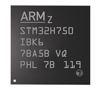 STM32H750IB资料手册解读:参数分析、引脚说明、应用示例介绍
 SG3525资料手册详解:SG3525参数分析、引脚说明、应用介绍
工作时间:9:00-21:00
CEO邮箱:ceo@jiepei.com
投诉邮箱:tousu@jiepei.com


 浙公网安备 33010502006866号 浙ICP备10014259号-119
营业执照ICP证
浙公网安备 33010502006866号 浙ICP备10014259号-119
营业执照ICP证


