AD6636
GENERAL TIMING CHARACTERISTICS
Table 3. General Timing Characteristics1, 2
Parameter
Temp
Test Level
Min
Typ
Max
Unit
CLK TIMING REQUIREMENTS
tCLK
tCLKL
tCLKH
tCLKSKEW
CLKx Period (x = A, B, C, D)
Full
Full
Full
Full
Full
Full
Full
Full
Full
Full
I
6.66
1.71
1.70
tCLK − 1.3
ns
ns
ns
ns
CLKx Width Low (x = A, B, C, D)
CLKx Width High (x = A, B, C, D)
CLKA to CLKx Skew (x = B, C, D)
IV
IV
IV
IV
IV
IV
IV
IV
IV
0.5 × tCLK
0.5 × tCLK
INPUT WIDEBAND DATA TIMING REQUIREMENTS
tSI
0.75
1.13
3.37
1.11
5.98
ns
ns
ns
ns
ns
INx [15:0] to ↑CLKx Setup Time (x = A, B, C, D)
INx [15:0] to ↑CLKx Hold Time (x = A, B, C, D)
EXPx [2:0] to ↑CLKx Setup Time (x = A, B, C, D)
EXPx [2:0] to ↑CLKx Hold Time (x = A, B, C, D)
↑CLKx to EXPx[2:0] Delay (x = A, B, C, D)
tHI
tSEXP
tHEXP
tDEXP
10.74
PARALLEL OUTPUT PORT TIMING REQUIREMENTS (MASTER)
tDPREQ
tDPP
Full
Full
Full
Full
Full
Full
Full
IV
IV
IV
IV
IV
IV
IV
1.77
2.07
0.48
0.38
0.23
4.59
0.90
3.86
5.29
5.49
5.35
4.95
ns
ns
ns
ns
ns
ns
ns
↑PCLK to ↑Px REQ Delay (x = A, B, C)
↑PCLK to Px [15:0] Delay (x = A, B, C)
↑PCLK to Px IQ Delay (x = A, B, C)
tDPIQ
tDPCH
tDPGAIN
tSPA
↑PCLK to Px CH[2:0] Delay (x = A, B, C)
↑PCLK to Px Gain Delay (x = A, B, C)
Px ACK to ↑PCLK Setup Time (x = A, B, C)
Px ACK to ↑PCLK Hold Time (x = A, B, C)
tHPA
PARALLEL OUTPUT PORT TIMING REQUIREMENTS (SLAVE)
tPCLK
tPCLKL
tPCLKH
tDPREQ
tDPP
PCLK Period
PCLK Low Period
PCLK High Period
Full
Full
Full
Full
Full
Full
Full
Full
Full
Full
IV
IV
IV
IV
IV
IV
IV
IV
IV
IV
5.0
1.7
0.7
4.72
4.8
ns
ns
ns
ns
ns
ns
ns
ns
ns
ns
0.5 × tPCLK
0.5 × tPCLK
8.87
↑PCLK to ↑Px REQ Delay (x = A, B, C)
↑PCLK to Px [15:0] Delay (x = A, B, C)
↑PCLK to Px IQ Delay (x = A, B, C)
↑PCLK to Px CH[2:0] Delay (x = A, B, C)
↑PCLK to Px Gain Delay (x = A, B, C)
Px ACK to ↓PCLK Setup Time (x = A, B, C)
Px ACK to ↓PCLK Hold Time (x = A, B, C)
8.48
tDPIQ
tDPCH
tDPGAIN
tSPA
4.83
4.88
5.08
6.09
1.0
10.94
10.09
11.49
tHPA
MISC PINS TIMING REQUIREMENTS
tRESET
tDIRP
tSS
RESET Width Low
Full
Full
Full
Full
IV
V
30
ns
ns
ns
ns
CPUCLK/SCLK to IRP Delay
SYNC(0, 1, 2, 3) to ↑CLKA Setup Time
SYNC(0, 1, 2, 3) to ↑CLKA Hold Time
7.5
IV
IV
0.87
0.67
tHS
1 All timing specifications are valid over the VDDCORE range of 1.7 V to 1.9 V and the VDDIO range of 3.0 V to 3.6 V.
2 CLOAD = 40 pF on all outputs, unless otherwise noted.
Rev. 0 | Page 6 of 72


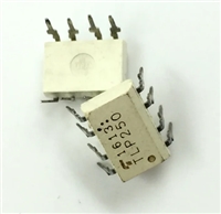
 TLP250光耦合器:资料手册参数分析

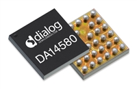
 DA14580 低功耗蓝牙系统级芯片(SoC):资料手册参数分析

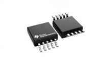
 INA226 高精度电流和功率监控器:资料手册参数分析

 SI2302 N沟道MOSFET:资料手册参数分析
