
 5秒后页面跳转

| 是否无铅: | 不含铅 | 是否Rohs认证: | 符合 |
| 生命周期: | Obsolete | 零件包装代码: | TSSOP |
| 包装说明: | ROHS COMPLIANT, MO-193BA, TSOT-8 | 针数: | 8 |
| Reach Compliance Code: | unknown | ECCN代码: | EAR99 |
| HTS代码: | 8542.39.00.01 | 风险等级: | 5.66 |
| Is Samacsys: | N | 转换器类型: | D/A CONVERTER |
| 输入位码: | BINARY | 输入格式: | SERIAL |
| JESD-30 代码: | R-PDSO-G8 | JESD-609代码: | e4 |
| 长度: | 2.9 mm | 最大线性误差 (EL): | 0.0977% |
| 湿度敏感等级: | 1 | 位数: | 8 |
| 功能数量: | 1 | 端子数量: | 8 |
| 最高工作温度: | 125 °C | 最低工作温度: | -40 °C |
| 封装主体材料: | PLASTIC/EPOXY | 封装代码: | VSSOP |
| 封装等效代码: | TSSOP8,.1 | 封装形状: | RECTANGULAR |
| 封装形式: | SMALL OUTLINE, VERY THIN PROFILE, SHRINK PITCH | 峰值回流温度(摄氏度): | 260 |
| 电源: | 3/5 V | 认证状态: | Not Qualified |
| 座面最大高度: | 1 mm | 最大稳定时间: | 0.11 µs |
| 标称安定时间 (tstl): | 0.016 µs | 子类别: | Other Converters |
| 最大压摆率: | 0.01 mA | 标称供电电压: | 3.5 V |
| 表面贴装: | YES | 技术: | CMOS |
| 温度等级: | AUTOMOTIVE | 端子面层: | Nickel/Palladium/Gold (Ni/Pd/Au) |
| 端子形式: | GULL WING | 端子节距: | 0.65 mm |
| 端子位置: | DUAL | 处于峰值回流温度下的最长时间: | 40 |
| 宽度: | 1.6 mm | Base Number Matches: | 1 |
| 型号 | 品牌 | 描述 | 获取价格 | 数据表 |
| AD5450_15 | ADI | 8-/10-/12-/14-Bit High Bandwidth Multiplying DACs with Serial Interface |
获取价格 |

|
| AD5450YUJ | ADI | 8/10/12/14-Bit High Bandwidth Multiplying DACs with Serial Interface |
获取价格 |
|
| AD5450YUJ-REEL7 | ADI | IC SERIAL INPUT LOADING, 0.016 us SETTLING TIME, 8-BIT DAC, PDSO8, MO-193BA, TSOT-8, Digit |
获取价格 |
|
| AD5450YUJZ-REEL | ADI | 8-/10-/12-/14-Bit High Bandwidth Multiplying DACs with Serial Interface |
获取价格 |
|
| AD5450YUJZ-REEL7 | ADI | 8-/10-/12-/14-Bit High Bandwidth Multiplying DACs with Serial Interface |
获取价格 |
|
| AD5451 | ADI | 8/10/12/14-Bit High Bandwidth Multiplying DACs with Serial Interface |
获取价格 |
|
 ADXL345传感器工作原理、参数分析、引脚说明

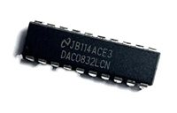 一文带你了解,DAC0832工作原理、输出电压范围、分辨率等参数
 ACS712电流检测使用指南及资料手册参数分析
 TLP521资料手册解读:参数分析、引脚说明、典型电路
工作时间:9:00-21:00
CEO邮箱:ceo@jiepei.com
投诉邮箱:tousu@jiepei.com


 浙公网安备 33010502006866号 浙ICP备10014259号-119
营业执照ICP证
浙公网安备 33010502006866号 浙ICP备10014259号-119
营业执照ICP证


