AD5303/AD5313/AD5323–SPECIFICATIONS
(VDD = +2.5 V to +5.5 V; VREF = +2 V; RL = 2 k⍀ to GND; CL = 200 pF to GND; all specifications TMIN to TMAX unless otherwise noted.)
B Version2
Typ
Parameter1
Min
Max
Units
Conditions/Comments
DC PERFORMANCE3, 4
AD5303
Resolution
8
Bits
LSB
LSB
Relative Accuracy
Differential Nonlinearity
AD5313
0.15
0.02
1
0.25
Guaranteed Monotonic by Design Over All Codes
Guaranteed Monotonic by Design Over All Codes
Resolution
10
0.5
0.05
Bits
LSB
LSB
Relative Accuracy
Differential Nonlinearity
AD5323
3
0.5
Resolution
12
Bits
Relative Accuracy
Differential Nonlinearity
Offset Error
2
12
1
3
1
60
LSB
LSB
0.2
0.4
0.15
10
–12
–5
Guaranteed Monotonic by Design Over All Codes
See Figures 3 and 4
See Figures 3 and 4
% of FSR
% of FSR
mV
ppm of FSR/°C
ppm of FSR/°C
dB
Gain Error
Lower Deadband
Offset Error Drift5
Gain Error Drift5
Power Supply Rejection Ratio5
DC Crosstalk5
See Figures 3 and 4
–60
30
∆VDD = 10%
µV
DAC REFERENCE INPUTS5
VREF Input Range
1
0
VDD
VDD
V
V
MΩ
kΩ
Buffered Reference Mode
Unbuffered Reference Mode
Buffered Reference Mode
Unbuffered Reference Mode. 0–VREF Output Range,
Input Impedance = RDAC
VREF Input Impedance
>10
180
90
kΩ
Unbuffered Reference Mode. 0–2 VREF Output Range,
Input Impedance = RDAC
Reference Feedthrough
Channel-to-Channel Isolation
–90
–80
dB
dB
Frequency = 10 kHz
Frequency = 10 kHz
OUTPUT CHARACTERISTICS5
Minimum Output Voltage6
Maximum Output Voltage6
DC Output Impedance
0.001
VDD – 0.001
V mi
V max
Ω
n
This is a measure of the minimum and maximum
drive capability of the output amplifier.
0.5
50
20
2.5
5
Short Circuit Current
mA
mA
µs
VDD = +5 V
VDD = +3 V
Power-Up Time
Coming Out of Power-Down Mode. VDD = +5 V
Coming Out of Power-Down Mode. VDD = +3 V
µs
LOGIC INPUTS5
Input Current
VIL, Input Low Voltage
1
µA
V
V
0.8
0.6
0.5
VDD = +5 V 10%
VDD = +3 V 10%
VDD = +2.5 V
V
VIH, Input High Voltage
Pin Capacitance
LOGIC OUTPUT (SDO)5
VDD = +5 V 10%
Output Low Voltage
Output High Voltage
VDD = +3 V 10%
Output Low Voltage
2.4
2.1
2.0
V
V
V
pF
VDD = +5 V 10%
VDD = +3 V 10%
VDD = +2.5 V
2
3.5
0.4
V
V
ISINK = 2 mA
ISOURCE = 2 mA
4.0
2.4
0.4
1
V
V
µA
pF
ISINK = 2 mA
Output High Voltage
Floating-State Leakage Current
Floating State O/P Capacitance
ISOURCE = 2 mA
DCEN = GND
DCEN = GND
3
POWER REQUIREMENTS
VDD
IDD (Normal Mode)
VDD = +4.5 V to +5.5 V
VDD = +2.5 V to +3.6 V
2.5
5.5
V
IDD Specification Is Valid for All DAC Codes
Both DACs Active and Excluding Load Currents
Both DACs in Unbuffered Mode. VIH = VDD and
VIL = GND. In Buffered Mode, extra current is
300
230
450
350
µA
µA
typically x µA per DAC where x = 5 µA + VREF/RDAC
.
IDD (Full Power-Down)
VDD = +4.5 V to +5.5 V
VDD = +2.5 V to +3.6 V
0.2
0.05
1
1
µA
µA
–2–
REV. 0


 CD4011双4位二进制计数器:资料手册参数分析

 PCM1794音频DAC:全面参数解析与关键特性指南

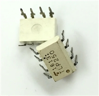
 TLP250光耦合器:资料手册参数分析

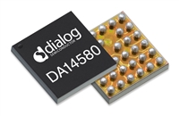
 DA14580 低功耗蓝牙系统级芯片(SoC):资料手册参数分析
