ICS9148-10
Technical Pin Function Descriptions
VDD(1,2,3)
48MHz(0:1)
This is the power supply to the internal core logic of the
device as well as the clock output buffers for REF(0:2),
PCICLK_F, PCICLK(0:6),48MHz0,48MHz1.
This is a fixed frequency Clock output that is typically used
to drive Super I/O devices. Outputs 0 and 1 are defined as
48MHz.
This pin operates at 3.3V volts. Clocks from the listed buffers
that it supplies will have a voltage swing from Ground to this
level. For the actual guaranteed high and low voltage levels
for the Clocks, please consult the DC parameter table in this
data sheet.
IOAPIC(0:1)
This Output is a fixed frequency Output Clock that runs at
the Reference Input (typically 14.31818MHz) . Its voltage
level swing is controlled by VDDL1 and may operate at 2.5 or
3.3volts.
VDDL1,2
REF(0:2)
This is the power supply for the CPUCLK (0:3) and IOAPIC
output buffers. The voltage level for these outputs may be
2.5 or 3.3volts. Clocks from the buffers that each supplies will
have a voltage swing from Ground to this level. For the actual
Guaranteed high and low voltage levels of these Clocks,
please consult the DC parameter table in this Data Sheet.
The REF Outputs are fixed frequency Clocks that run at the
same frequency as the Input Reference Clock X1 or the
Crystal (typically 14.31818MHz) attached across X1 and X2.
PCICLK_F
ThisOutputisequaltoPCICLK(0:6)andisFREERUNNING,
and will not be stopped by PCI_STOP#.
GND(1,2,3)
This is the ground to the internal core logic of the device as
well as the clock output buffers for REF(0:2), PCICLK_F,
PCICLK(0:6),48MHz0,48MHz1.
PCICLK(0:6)
These Output Clocks generate all the PCI timing requirements
for a Pentium/Pro based system. They conform to the current
PCI specification. They run at 33.3 MHz.
GNDL(1,2)
SELECT100/66.6MHz#
This is the ground for the CPUCLK (0:3) and IOAPIC output
buffers.
This Input pin controls the frequency of the Clocks at the
CPUCLK, PCICLK and SDRAM output pins. If a logic 1
valueispresentonthispin, the100MHzClockwillbeselected.
If a logic 0 is used, the 66.6MHz frequency will be selected.
The PCI clock is multiplexed to be 33.3MHz for both select
cases. PCI is synchronous at the rising edge of PCI to the
CPU rising edge (with the skew making CPU early).
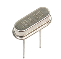
X1
This input pin serves one of two functions. When the device
is used with a Crystal, X1 acts as the input pin for the
reference signal that comes from the discrete crystal. When
the device is driven by an external clock signal, X1 is the
device input pin for that reference clock. This pin also
implements an internal Crystal loading capacitor that is
connected to ground. With a nominal value of 33pF no
external load cap is needed for a CL=17 to 18pF crystal.
PWR_DWN#
This is an asynchronous active Low Input pin used to Power
Down the device into a Low Power state by not removing the
power supply. The internal Clocks are disabled and the VCO
and Crystal are stopped. Powered Down will also place all
the Outputs in a low state at the end of their current cycle.
The latency of Power Down will not be greater than 3ms.
X2
This Output pin is used only when the device uses a Crystal
as the reference frequency source. In this mode of operation,
X2 is an output signal that drives (or excites) the discrete
Crystal. The X2 pin will also implement an internal Crystal
loading capacitor nominally 33pF.
CPU_STOP#
This is a synchronous active Low Input pin used to stop the
CPUCLK clocks in an active low state. All other Clocks
including SDRAM clocks will continue to run while this
function is enabled. The CPUCLKs will have a turn ON
latency of at least 3 CPU clocks.
CPUCLK(0:3)
These Output pins are the Clock Outputs that drive processor
and other CPU related circuitry that requires clocks which are
in tight skew tolerance with the CPU clock. The voltage
swing of these Clocks is controlled by the Voltage level
applied to the VDDL2 pin of the device. See the Functionality
Table for a list of the specific frequencies that are available
for these Clocks and the selection codes to produce them.
PCI_STOP#
This is a synchronous active Low Input pin used to stop the
PCICLK clocks in an active low state. It will not affect
PCICLK_F nor any other outputs.
3


 资料手册解读:UC3842参数和管脚说明

 一文带你了解无源晶振的负载电容为何要加两颗谐振电容CL1和CL2

 玻璃管保险丝与陶瓷管保险丝:区别与替代性探讨

 PCF8574资料解读:主要参数分析、引脚说明
