6
AC Electrical Specifications
Over recommended operating conditions (T = –55˚C to +125˚C, V
= 0 V, V
= 0 V, V
= 5 V and
A
IN+
IN–
DD1
V
= 5 V, unless otherwise specified).
DD2
[12]
Group A
Symbol Subgroups Min. Typ.* Max. Units
Parameter
Test Conditions
Fig. Note
16 8,13
Common Mode
Rejection
CMR
9
5
8
kV/
V
= 1 kV
CM
µs
4.5 V ≤ (V
, V
DD1 DD2
)
≤ 5.5 V, T = 25˚C
A
Propagation
Delay to 50%
t
9,10,11
3.7
7.5
µs
V
= 0 to 100 mV step 18,19
IN+
PD50
PD90
4.5 V ≤ (V
≤ 5.5 V
, V
DD1 DD2
)
Propagation
Delay to 90%
t
9,10,11
9,10,11
9,10,11
5.7
3.4
11.0
7.5
Rise/Fall
Time (10-90%)
t
R/F
Small-Signal
Bandwidth
(–3 dB)
f
45
100
kHz 4.5 V ≤ (V
≤ 5.5 V
, V
DD1 DD2
)
18,20, 14
21
–3 dB
V
= 200 mVpk-pk
IN+
sine wave
Small-Signal
Bandwidth
(–45˚)
f
31
–45˚
RMS Input-
Referred Noise
V
0.6
mV
mV
In recommended
application circuit
22,24
9
N
rms
Power Supply
Rejection
PSR
570
10
P–P
*All typicals are at the nominal operating conditions of V
= 0 V, V
= 0 V, T = 25˚C, V
= 5 V and V
= 5 V.
IN+
IN–
A
DD1
DD2
Notes:
1. If V
is brought above V
–2 V with respect to GND1 an internal test mode may be activated. This test mode is not intended for
IN–
DD1
customer use.
2. Exact offset value is dependent on layout of external bypass capacitors. The offset value in the data sheet corresponds to Agilent’s
recommended layout (see Figures 26 and 27).
3. Nonlinearity is defined as half of the peak-to-peak output deviation from the best-fit gain line, expressed as a percentage of the full-scale
differential output voltage.
4. Because of the switched capacitor nature of the sigma-delta A/D converter, time averaged values are shown.
5. CMRR is defined as the ratio of the gain for differential inputs applied between pins 2 and 3 to the gain for both common mode inputs
IN
applied to both pins 2 and 3 with respect to pin 4.
6. When the differential input signal exceeds approximately 320 mV, the outputs will limit at the typical values shown.
7. Short-circuit current is the amount of output current generated when either output is shorted to V
recommend operations under these conditions.
or ground. Agilent does not
DD2
8. CMR (also known as IMR or Isolation Mode Rejection) specifies the minimum rate of rise of a common mode signal applied across the
isolation boundary at which small output perturbations begin to occur. These output perturbations can occur with both the rising and
falling edges of the common mode waveform and may be of either polarity. A CMR failure is defined as a perturbation exceeding 200 mV
at the output of the recommended application circuit (Figure 24). See Applications section for more information on CMR.
9. Output noise comes from two primary sources: chopper noise and sigma-delta quantization noise. Chopper noise results from chopper
stabilization of the output op-amps. It occurs at a specific frequency (typically 500 kHz) and is not attenuated by the on-chip output
filter. The on-chip filter does eliminate most, but not all, of the sigma-delta quantization noise. An external filter circuit may be easily
added to the external post-amplifier to reduce the total RMS output noise. See Applications section for more information.
10. Data sheet value is the amplitude of the transient at the differential output of the HCPL-7850 when a 1 V , 1 MHz square wave with
P–P
100 ns rise and fall times (measured at pins 1 and 8) is applied to both V
and V
.
DD1
DD2
11. Device considered a two-terminal device: Pins 1, 2, 3, and 4 are shorted together and pins 5, 6, 7, and 8 are shorted together.
12. Commercial parts receive 100% testing at 25˚C (Subgroups 1 and 9). Hi-Rel and SMD parts receive 100% testing at 25˚C, +125˚C and
–55˚C (Subgroups 1 and 9, 2 and 10, 3 and 11, respectively).
13. Parameters are tested as part of device initial characterization and after design and process changes only. Parameters are guaranteed to
limits specified for all lots not specifically tested.
14. The f
test is guaranteed by the T
test.
RISE
-3dB


 ?TPA3116D2功放芯片参数详解、引脚说明

 74HC165引脚说明、驱动程序示例解读

 深入解析AD9833:DDS频率合成器的卓越性能与广泛应用

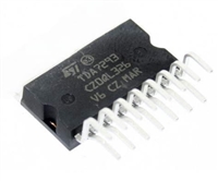
 高性能TDA7293音频功率放大器技术特性与应用分析
