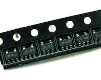
AD767
THE AD767 OFFERS TRUE 12-BIT PERFORMANCE
OVER THE FULL TEMPERATURE RANGE
Gain and offset drift are minimized in the AD767 because of the
thermal tracking of the scaling resistors with other device
components. Connections for various output voltage ranges are
shown in Table I.
LINEARITY ERROR: Analog Devices defines linearity error as
the maximum deviation of the actual, adjusted DAC output
from the ideal analog output (a straight line drawn from 0 to
F.S. – 1 LSB) for any bit combination. This is also referred to as
relative accuracy. The AD767 is laser trimmed to typically
maintain linearity errors at less than ±1/8 LSB for the K and B
versions and ±1/2 LSB for the J, A and S versions. Linearity
over temperature is also held to ±1/2 LSB (K/B) or ±1 LSB
(J/A/S).
MONOTONICITY: A DAC is said to be monotonic if the
output either increases or remains constant for increasing digital
inputs such that the output will always be a nondecreasing
function of input. All versions of the AD767 are monotonic over
their full operating temperature range.
Figure 1. Output Amplifier Voltage Range Scaling Circuit
UNIPOLAR CONFIGURATION (Figure 2)
DIFFERENTIAL NONLINEARITY: Monotonic behavior
requires that the differential linearity error be less than 1 LSB
both at +25°C as well as over the temperature range of interest.
Differential nonlinearity is the measure of the variation in analog
value, normalized to full scale, associated with a 1 LSB change
in digital input code. For example, for a 10 volt full-scale
output, a change of 1 LSB in digital input code should result in
a 2.44 mV change in the analog output (1 LSB = 10 V ϫ
1/4096 = 2.44 mV). If in actual use, however, a 1 LSB change
in the input code results in a change of only 0.61 mV (1/4 LSB)
in analog output, the differential nonlinearity error would be
–1.83 mV, or –3/4 LSB.
This configuration will provide a unipolar 0 to +10 volt output
range. In this mode, the bipolar offset terminal, Pin 4, should be
grounded if not used for trimming.
STEP I … ZERO ADJUST
Turn all bits OFF and adjust zero trimmer R1, until the output
reads 0.000 volts (1 LSB = 2.44 mV). In most cases this trim is
not needed, and Pin 4 should be connected to Pin 5.
STEP II … GAIN ADJUST
Turn all bits ON and adjust 100 Ω gain trimmer R2 until the
output is 9.9976 volts. (Full scale is adjusted to 1 LSB less than
nominal full scale of 10.000 volts.)
GAIN ERROR: DAC gain error is a measure of the difference
between an ideal DAC and the actual device’s output span. All
grades of the AD767 have a maximum gain error of 0.2% FS.
However, if this is not sufficient, the error can easily be adjusted
to zero (see Figures 2 and 3).
UNIPOLAR OFFSET ERROR: Unipolar offset error is a
combination of the offset errors of the voltage-mode DAC and
the output amplifier and is measured when the AD767 is
configured for unipolar outputs. It is present for all codes and is
measured with all “0s” in the DAC latches. This is easily
adjustable to zero when required.
BIPOLAR ZERO ERROR: Bipolar zero errors result from
errors produced by the DAC and output amplifier when the
AD767 is configured for bipolar output. Again, as with unipolar
offset and gain errors, this is easily adjusted to zero when
required.
Figure 2. 0 to +10 V Unipolar Voltage Output
ANALOG CIRCUIT CONNECTIONS
Internal scaling resistors provided in the AD767 may be connected
to produce bipolar output voltage ranges of ±10, ±5 or ±2.5 V
or unipolar output voltage ranges of 0 to +5 V or 0 to+10 V.
Table I. Output Voltage Range Connections
Output
Range
Digital
Input Codes
Connect
Pin 9 to
Connect
Pin 1 to
Connect
Pin 2 to
Connect
Pin 4 to
±10 V
±5 V
±2.5 V
0 to +10 V
0 to +5 V
Offset Binary
Offset Binary
Offset Binary
Straight Binary
Straight Binary
1
9
NC
1 and 9
9
1 and 9
9
6 (through 50 Ω fixed or 100 Ω trim resistor)
6 (through 50 Ω fixed or 100 Ω trim resistor)
6 (through 50 Ω fixed or 100 Ω trim resistor)
5 (or optional trim – See Figure 2)
1 and 2
2
1 and 2
2
2 and 9
3
2 and 9
3
5 (or optional trim – See Figure 2)
–4–
REV. A


 一文带你解读74HC244资料手册:特性、应用场景、封装方式、引脚配置说明、电气参数、推荐替代型号

 AD623资料手册解读:特性、应用、封装、引脚功能及电气参数

 RT9193资料手册解读:RT9193引脚功能、电气参数、替换型号推荐

 VIPER22A的资料手册解读、引脚参数说明、代换型号推荐
