
 5秒后页面跳转

| 型号 | 品牌 | 获取价格 | 描述 | 数据表 |
| W3DG6463V75D2-M | WEDC |
获取价格 |
Synchronous DRAM Module, 64MX64, 5.4ns, CMOS, DIMM-168 |

|
| W3DG6463V75D2-M | MICROSEMI |
获取价格 |
Synchronous DRAM Module, 64MX64, 5.4ns, CMOS, DIMM-168 |
|
| W3DG6463V75D2-MG | WEDC |
获取价格 |
Synchronous DRAM Module, 64MX64, 5.4ns, CMOS, ROHS COMPLIANT, DIMM-168 |
|
| W3DG6463V75D2-MG | MICROSEMI |
获取价格 |
Synchronous DRAM Module, 64MX64, 5.4ns, CMOS, ROHS COMPLIANT, DIMM-168 |
|
| W3DG6463V75D2-S | MICROSEMI |
获取价格 |
Synchronous DRAM Module, 64MX64, 5.4ns, CMOS, DIMM-168 |
|
| W3DG6463V75D2-SG | MICROSEMI |
获取价格 |
Synchronous DRAM Module, 64MX64, 5.4ns, CMOS, ROHS COMPLIANT, DIMM-168 |
|
| W3DG6463V75D2-X | WEDC |
获取价格 |
512MB - 2x32Mx64 SDRAM UNBUFFERED |
|
| W3DG6463V7D2-G | WEDC |
获取价格 |
512MB - 2x32Mx64 SDRAM UNBUFFERED |
|
| W3DG6463V7D2-G | MICROSEMI |
获取价格 |
Synchronous DRAM Module, 64MX64, 5.4ns, CMOS, DIMM-168 |
|
| W3DG6463V7D2-GG | MICROSEMI |
获取价格 |
Synchronous DRAM Module, 64MX64, 5.4ns, CMOS, ROHS COMPLIANT, DIMM-168 |
|
 SZNUP2105LT1G电气参数、产品特性详解

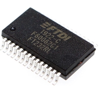 FT232RL资料解读:引脚说明、参数详情、产品特性
 RC0402FR-07100KL资料解读:电气参数、产品特性
 RC0603FR-070R数据手册解读:特性、应用与替换型号推荐
工作时间:9:00-21:00
CEO邮箱:ceo@jiepei.com
投诉邮箱:tousu@jiepei.com


 浙公网安备 33010502006866号 浙ICP备10014259号-119
营业执照ICP证
浙公网安备 33010502006866号 浙ICP备10014259号-119
营业执照ICP证


