
| 型号 | 品牌 | 获取价格 | 描述 | 数据表 |
| U62H256SK35 | ETC |
获取价格 |
x8 SRAM |

|
| U62H256SK55 | ETC |
获取价格 |
x8 SRAM |
|
| U62H64 | ZMD |
获取价格 |
AUTOMOTIVE FAST 8K X 8 SRAM |
|
| U62H64JC35L | IDT |
获取价格 |
Standard SRAM, 8KX8, 35ns, CMOS, PDSO28 |
|
| U62H64JK20 | IDT |
获取价格 |
Standard SRAM, 8KX8, 20ns, CMOS, PDSO28 |
|
| U62H64JK20L | IDT |
获取价格 |
Standard SRAM, 8KX8, 20ns, CMOS, PDSO28 |
|
| U62H64JK25 | IDT |
获取价格 |
暂无描述 |
|
| U62H64JK25L | IDT |
获取价格 |
Standard SRAM, 8KX8, 25ns, CMOS, PDSO28 |
|
| U62H64JK35 | IDT |
获取价格 |
Standard SRAM, 8KX8, 35ns, CMOS, PDSO28 |
|
| U62H64JK35L | IDT |
获取价格 |
Standard SRAM, 8KX8, 35ns, CMOS, PDSO28 |
|
 博通斩获OpenAI百亿订单,能否撼动英伟达AI芯片霸主地位

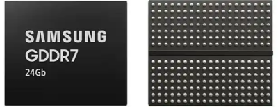 英伟达追加GDDR7显存订单 三星紧急扩产应对AI芯片需求激增
 东莞AI潮玩签下亿元出海大单 国产芯片借势加速普及
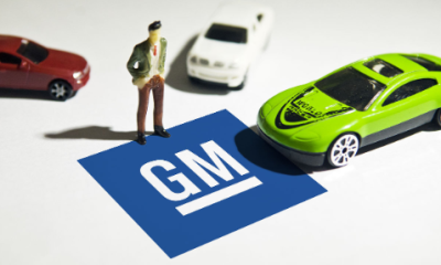 通用汽车大举收缩美国电动车产能 行业寒冬或已来临
工作时间:9:00-21:00
CEO邮箱:ceo@jiepei.com
投诉邮箱:tousu@jiepei.com


 浙公网安备 33010502006866号 浙ICP备10014259号-119
营业执照ICP证
浙公网安备 33010502006866号 浙ICP备10014259号-119
营业执照ICP证


