ꢀ ꢁꢂ ꢃ ꢃꢄ ꢃ ꢅꢆꢇ
ꢈꢅ ꢉꢊ ꢀꢋ ꢄ ꢃ ꢌ ꢍꢎꢍꢋ ꢁꢏ ꢐꢅꢎ ꢏꢐ ꢑ ꢒ ꢓꢔ ꢓꢁ ꢏꢕ ꢅꢀꢏ ꢅꢖꢊꢕ ꢊ ꢀꢓꢁ ꢗꢏ ꢔꢂꢑ ꢒꢀ ꢑꢒ
SGLS230A − JANUARY 2004 − REVISED JUNE 2008
Terminal Functions
TERMINAL
I/O
DESCRIPTION
NAME
AIN
NO.
26
I
I
Analog input
AV
AV
16, 27
18, 23, 28
17
Analog supply voltage
Analog ground
DD
I
SS
BG
O
Band gap reference voltage. A 1-µF capacitor (with an optional 0.1-µF capacitor in parallel) should be
connected between this terminal and AV for external filtering.
SS
Clock input. The input is sampled on each rising edge of CLK.
Common mode level. This voltage is equal to (AV − AV ) ÷ 2. An external 0.1-µF capacitor should be
CLK
CML
12
25
I
O
DD SS
connected between this terminal and AV
.
SS
D0 − D7
2 − 9
1
O
I
Data outputs. D7 is the MSB.
DRV
DRV
Supply voltage for digital output drivers
Ground for digital output drivers
Digital supply voltage
DD
10
14
13
11
I
SS
DV
OE
DV
I
DD
I
Output enable. When high, the D0 − D7 outputs go in high-impedance mode.
Digital ground
I
SS
PWDN_REF
REFBI
24
21
I
Power down for internal reference voltages. A high on this terminal disables the internal reference circuit.
I
Reference voltage bottom input. The voltage at this terminal defines the bottom reference voltage for the
ADC. It can be connected to REFBO or to an externally generated reference level. Sufficient filtering
should be applied to this input. The use of a 0.1-µF capacitor connected between REFBI and AV
recommended. Additionaly, a 0.1-µF capacitor can be connected between REFTI and REFBI.
is
SS
REFBO
REFTI
22
20
O
I
Reference voltage bottom output. An internally generated reference is available at this terminal. It can be
connected to REFBI or left unconnected. A 1-µF capacitor between REFBO and AV
provides sufficient
SS
decoupling required for this output.
Reference voltage top input. The voltage at this terminal defines the top reference voltage for the ADC.
It can be connected to REFTO or to an externally generated reference level. Sufficient filtering should be
applied to this input. The use of a 0.1-µF capacitor between REFTI and AV
Additionaly, a 0.1-µF capacitor can be connected between REFTI and REFBI.
is recommended.
SS
REFTO
STBY
19
15
O
I
Reference voltage top output. An internally generated reference is available at this terminal. It can be
connected to REFTI or left unconnected. A 1-µF capacitor between REFTO and AV
provides sufficient
SS
decoupling required for this output.
Standby input. A high level on this input enables power-down mode.
†
absolute maximum ratings over operating free-air temperature (unless otherwise noted)
Supply voltage range: AV
AV
Digital input voltage range to DV
Analog input voltage range to AV
Digital output voltage range applied from external source to DGND . . . . . . . . . . . . . . −0.5 V to DV
Reference voltage input range to AGND: V , V , V , V −0.5 V to AV
to AV , DV
to DV
. . . . . . . . . . . . . . . . . . . . . . . . . . . . . . . . . . −0.5 V to 4.5 V
. . . . . . . . . . . . . . . . . . . . . . . . . . . . . . . . . . −0.5 V to 0.5 V
DD
DD
SS
DD
SS
SS
SS
to DV , AV to DV
DD
SS
SS
. . . . . . . . . . . . . . . . . . . . . . . . . . . . . . . . . . . . . . . . . . −0.5 V to DV
. . . . . . . . . . . . . . . . . . . . . . . . . . . . . . . . . . . . . . . . . −0.5 V to AV
+ 0.5 V
+ 0.5 V
+ 0.5 V
+ 0.5 V
DD
DD
DD
DD
(REFTI) (REFTO) (REFBI) (REFBO)
Operating free-air temperature range, T : TLV5535I . . . . . . . . . . . . . . . . . . . . . . . . . . . . . . . . . . −40°C to 85°C
A
Storage temperature range, T
. . . . . . . . . . . . . . . . . . . . . . . . . . . . . . . . . . . . . . . . . . . . . . . . . . . −55°C to 150°C
stg
†
Stresses beyond those listed under “absolute maximum ratings” may cause permanent damage to the device. These are stress ratings only, and
functional operation of the device at these or any other conditions beyond those indicated under “recommended operating conditions” is not
implied. Exposure to absolute-maximum-rated conditions for extended periods may affect device reliability.
4
POST OFFICE BOX 655303 • DALLAS, TEXAS 75265


 MAX6675资料手册参数详解、引脚配置说明

 LM258引脚图及功能介绍、主要参数分析

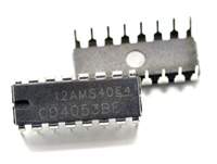
 CD4052资料手册参数详解、引脚配置说明

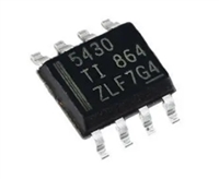
 一文带你了解TPS5430资料手册分析:参数介绍、引脚配置说明
