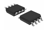
5秒后页面跳转
TLC274_V01 PDF预览

TLC274_V01

更新时间: 2024-01-04 04:29:52
品牌 Logo 应用领域
德州仪器 - TI 放大器
页数 文件大小 规格书
49页 1496K
描述
LinCMOS PRECISION QUAD OPERATIONAL AMPLIFIERS

TLC274_V01 数据手册

 浏览型号TLC274_V01的Datasheet PDF文件第2页浏览型号TLC274_V01的Datasheet PDF文件第3页浏览型号TLC274_V01的Datasheet PDF文件第4页浏览型号TLC274_V01的Datasheet PDF文件第5页浏览型号TLC274_V01的Datasheet PDF文件第6页浏览型号TLC274_V01的Datasheet PDF文件第7页 
ꢀ ꢁꢂ ꢃ ꢄ ꢅꢆ ꢀ ꢁꢂ ꢃ ꢄ ꢅꢇ ꢆ ꢀ ꢁꢂ ꢃ ꢄ ꢅꢈ ꢆ ꢀ ꢁꢂ ꢃ ꢄ ꢅ ꢉꢆ ꢀꢁ ꢂꢃ ꢄꢊ  
ꢐꢑꢒ ꢂꢓꢏ ꢓꢎ ꢔ ꢕ ꢖꢇꢗ ꢎ ꢐꢒꢑ ꢇꢀ ꢓꢎ ꢔꢇꢁ ꢇꢍ ꢐ ꢁꢓ ꢘꢓ ꢒꢑ ꢏ  
ꢁꢋ  
SLOS092D − SEPTEMBER 1987 − REVISED MARCH 2001  
D
Trimmed Offset Voltage:  
TLC279 . . . 900 µV Max at 25°C,  
= 5 V  
D, J, N, OR PW PACKAGE  
(TOP VIEW)  
V
DD  
D
D
Input Offset Voltage Drift . . . Typically  
0.1 µV/Month, Including the First 30 Days  
Wide Range of Supply Voltages Over  
Specified Temperature Range:  
0°C to 70°C . . . 3 V to 16 V  
−40°C to 85°C . . . 4 V to 16 V  
−55°C to 125°C . . . 4 V to 16 V  
Single-Supply Operation  
1OUT  
1IN−  
1IN+  
4OUT  
13 4IN−  
1
2
3
4
5
6
7
14  
12  
11  
10  
9
4IN+  
GND  
3IN+  
3IN−  
3OUT  
V
DD  
2IN+  
2IN−  
8
2OUT  
D
D
Common-Mode Input Voltage Range  
Extends Below the Negative Rail (C-Suffix  
and I-Suffix Versions)  
FK PACKAGE  
(TOP VIEW)  
D
D
D
D
D
Low Noise . . . Typically 25 nV/Hz  
at f = 1 kHz  
3
2
1
20 19  
18  
Output Voltage Range Includes Negative  
Rail  
4IN+  
NC  
1IN+  
NC  
4
5
6
7
8
17  
16  
15  
14  
12  
High Input Impedance . . . 10 Typ  
GND  
NC  
V
DD  
NC  
ESD-Protection Circuitry  
3IN+  
2IN+  
Small-Outline Package Option Also  
Available in Tape and Reel  
9 10 11 12 13  
D
Designed-In Latch-Up Immunity  
description  
NC − No internal connection  
The TLC274 and TLC279 quad operational  
amplifiers combine a wide range of input offset  
voltage grades with low offset voltage drift, high  
input impedance, low noise, and speeds  
approaching that of general-purpose BiFET  
devices.  
DISTRIBUTION OF TLC279  
INPUT OFFSET VOLTAGE  
30  
25  
20  
15  
10  
5
290 Units Tested From 2 Wafer Lots  
= 5 V  
V
T
A
DD  
= 25°C  
These devices use Texas Instruments silicon-  
gate LinCMOStechnology, which provides  
offset voltage stability far exceeding the stability  
N Package  
available  
with  
conventional  
metal-gate  
processes.  
The extremely high input impedance, low bias  
currents, and high slew rates make these  
cost-effective devices ideal for applications which  
have previously been reserved for BiFET and  
NFET products. Four offset voltage grades are  
available (C-suffix and I-suffix types), ranging  
from the low-cost TLC274 (10 mV) to the high-  
precision TLC279 (900 µV). These advantages, in  
combination with good common-mode rejection  
and supply voltage rejection, make these devices  
a good choice for new state-of-the-art designs as  
well as for upgrading existing designs.  
0
1200  
600  
0
600  
1200  
V
IO  
− Input Offset Voltage − µV  
LinCMOS is a trademark of Texas Instruments.  
ꢀꢢ  
Copyright 2001, Texas Instruments Incorporated  
ꢞ ꢢ ꢟ ꢞꢋ ꢌꢬ ꢚꢙ ꢝ ꢥꢥ ꢣꢝ ꢛ ꢝ ꢜ ꢢ ꢞ ꢢ ꢛ ꢟ ꢧ  
ꢠꢢ  
ꢝꢛ  
1
POST OFFICE BOX 655303 DALLAS, TEXAS 75265  

与TLC274_V01相关器件

型号 品牌 获取价格 描述 数据表
TLC274A TI

获取价格

LinCMOSE PRECISION QUAD OPERATIONAL AMPLIFIERS
TLC274ACD TI

获取价格

LinCMOSE PRECISION QUAD OPERATIONAL AMPLIFIERS
TLC274ACD ROCHESTER

获取价格

QUAD OP-AMP, 6500uV OFFSET-MAX, 1.7MHz BAND WIDTH, PDSO14, GREEN, PLASTIC, MS-012AB, SOIC-
TLC274ACDG4 TI

获取价格

The TLC274 and TLC279 quad operational amplifiers combine a wide range of input offset vol
TLC274ACDP3 TI

获取价格

IC OP-AMP, Operational Amplifier
TLC274ACDR TI

获取价格

The TLC274 and TLC279 quad operational amplifiers combine a wide range of input offset vol
TLC274ACDR ROCHESTER

获取价格

QUAD OP-AMP, 6500uV OFFSET-MAX, 1.7MHz BAND WIDTH, PDSO14, GREEN, PLASTIC, MS-012AB, SOIC-
TLC274ACDRG4 TI

获取价格

The TLC274 and TLC279 quad operational amplifiers combine a wide range of input offset vol
TLC274ACJ TI

获取价格

QUAD OP-AMP, 6500uV OFFSET-MAX, 2.2MHz BAND WIDTH, CDIP14
TLC274ACJP4 TI

获取价格

IC OP-AMP, Operational Amplifier