
| 是否Rohs认证: | 符合 | 生命周期: | Active |
| Reach Compliance Code: | unknown | 风险等级: | 5.71 |
| 峰值回流温度(摄氏度): | 260 | 处于峰值回流温度下的最长时间: | 40 |
| uPs/uCs/外围集成电路类型: | CLOCK GENERATOR, PROCESSOR SPECIFIC | Base Number Matches: | 1 |
| 型号 | 品牌 | 获取价格 | 描述 | 数据表 |
| SI5346A-B05433-GM | SILICON |
获取价格 |

|
|
| SI5346A-B05854-GM | SKYWORKS |
获取价格 |
|
|
| SI5346A-B06216-GM | SKYWORKS |
获取价格 |
IC |
|
| SI5346A-D-GM | SILICON |
获取价格 |
Processor Specific Clock Generator, 712.5MHz, CMOS, QFN-44 |
|
| SI5346A-D06344-GMR | SKYWORKS |
获取价格 |
|
|
| SI5346A-D08273-GMR | SILICON |
获取价格 |
Processor Specific Clock Generator, |
|
| SI5346A-D09245-GM | SILICON |
获取价格 |
Processor Specific Clock Generator, |
|
| SI5346A-D09245-GMR | SILICON |
获取价格 |
Processor Specific Clock Generator, |
|
| Si5346B | SKYWORKS |
获取价格 |
QFN44 |
|
| SI5346B-A-GMR | SKYWORKS |
获取价格 |
最小工作电压(V):1.71V;最大工作电压(V):3.47V;最大输出频率(MHz):3 |
|
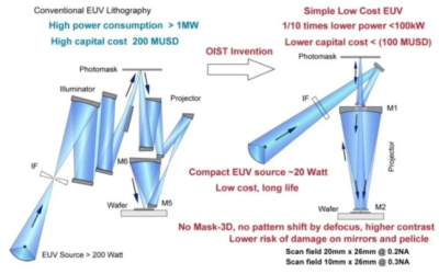 俄罗斯公布极紫外光刻机路线图 能否撼动ASML霸主地位?

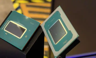 英特尔Panther Lake旗舰型号TDP升至45W,LPE核心首度开放调用权限
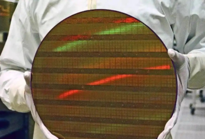 三星2nm晶圆代工降价三分之一 价格战能否撼动台积电霸主地位?
 Vuzix联袂TCL华星光电 突破AR眼镜光学显示技术瓶颈
工作时间:9:00-21:00
CEO邮箱:ceo@jiepei.com
投诉邮箱:tousu@jiepei.com


 浙公网安备 33010502006866号 浙ICP备10014259号-119
营业执照ICP证
浙公网安备 33010502006866号 浙ICP备10014259号-119
营业执照ICP证


