
| 型号 | 品牌 | 获取价格 | 描述 | 数据表 |
| PD2503 | NIEC |
获取价格 |
250A Avg 300 800 Volts |

|
| PD2504 | NIEC |
获取价格 |
250A Avg 300 800 Volts |
|
| PD2508 | NIEC |
获取价格 |
250A Avg 300 800 Volts |
|
| PD2508 | KYOCERA AVX |
获取价格 |
本公司利用丰富的封装技术生产制造模块产品,并投放到工业和车载市场。现在社会要求有效用电,在 |
|
| PD250GB40 | SANREX |
获取价格 |
THYRISTOR MODULE |
|
| PD250GB80 | SANREX |
获取价格 |
THYRISTOR MODULE |
|
| PD250HB | SANREX |
获取价格 |
THYRISTOR MODULE |
|
| PD250HB120 | SANREX |
获取价格 |
THYRISTOR MODULE |
|
| PD250HB160 | SANREX |
获取价格 |
THYRISTOR MODULE |
|
| PD250KN16A | KYOCERA AVX |
获取价格 |
本公司利用丰富的封装技术生产制造模块产品,并投放到工业和车载市场。现在社会要求有效用电,在 |
|
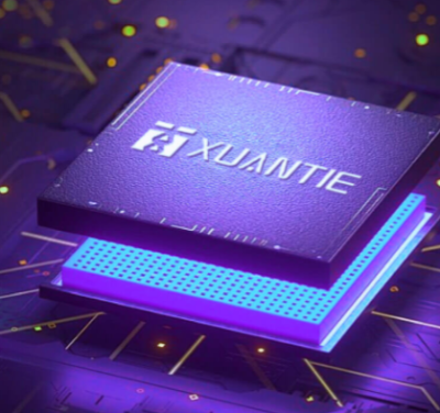 玄铁E901发布:全球最小RISC-V处理器如何颠覆嵌入式市

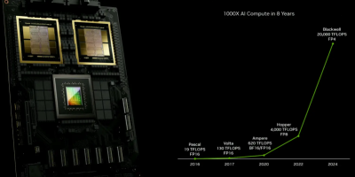 英伟达发布机器人"新大脑"芯片:物理AI或将重塑人机协作格局
 58年横滨工厂谢幕:尼康关厂背后的轻资产突围战
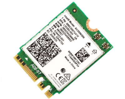 英特尔Wi-Fi 7新品BE213发布:三频160MHz频宽能否满足未来需求?
工作时间:9:00-21:00
CEO邮箱:ceo@jiepei.com
投诉邮箱:tousu@jiepei.com


 浙公网安备 33010502006866号 浙ICP备10014259号-119
营业执照ICP证
浙公网安备 33010502006866号 浙ICP备10014259号-119
营业执照ICP证


