Absolute Maximum Ratings:
Supply Voltage, V+ . . . . . . . . . . . . . . . . . . . . . . . . . . . . . . . . . . . . . . . . . . . . . . . . . . . . . . . . . 36V or ±18V
Differential Input Voltage (Note 1) . . . . . . . . . . . . . . . . . . . . . . . . . . . . . . . . . . . . . . . . . . . . . . . . . . . . 36V
Input Voltage . . . . . . . . . . . . . . . . . . . . . . . . . . . . . . . . . . . . . . . . . . . . . . . . . . . . . . . . . . . . . –0.3V to +36V
Power Dissipation (Note 2)
NTE943 . . . . . . . . . . . . . . . . . . . . . . . . . . . . . . . . . . . . . . . . . . . . . . . . . . . . . . . . . . . . . . . . . 660mW
NTE943M . . . . . . . . . . . . . . . . . . . . . . . . . . . . . . . . . . . . . . . . . . . . . . . . . . . . . . . . . . . . . . . 780mW
NTE943SM . . . . . . . . . . . . . . . . . . . . . . . . . . . . . . . . . . . . . . . . . . . . . . . . . . . . . . . . . . . . . . 510mW
Output Short Circuit to GND (Note 3) . . . . . . . . . . . . . . . . . . . . . . . . . . . . . . . . . . . . . . . . . . Continuous
Input Current (VIN < –0.3V), Note 4) . . . . . . . . . . . . . . . . . . . . . . . . . . . . . . . . . . . . . . . . . . . . . . . . 50mA
Operating Temperature Range . . . . . . . . . . . . . . . . . . . . . . . . . . . . . . . . . . . . . . . . . . . . . . . 0° to +70°C
Storage Temperature Range . . . . . . . . . . . . . . . . . . . . . . . . . . . . . . . . . . . . . . . . . . . . . . –65° to +150°C
Lead Temperature (During Soldering, 10 sec) . . . . . . . . . . . . . . . . . . . . . . . . . . . . . . . . . . . . . . +260°C
Note 1. Positive excursions of input voltage may exceed the power supply level. As long as the other
voltage remains within the common–mode range, the comparator will provide a proper out-
put state. The low input voltage state must not be less than –0.3V (or 0.3V below the the
magnitude of the negative power supply, if used).
Note 2. For operating at elevated temperature, these devices must be derated based on a 125°C
maximum junction temperature and a thermal resistance of 127°C/W which applies for the
device soldered in a printed circuit board, operating in a still air ambient. The low bias dis-
sipation and the “ON–OFF” haracteristic of the output keeps the chip dissipation very small
(PD ≤ 100mW), provided the output transistors are allowed to saturate.
Note 3. Short circuits from the output to V+ can cause excessive heating and eventual destruction.
When considering short circuits to GND, the maximum output current is approximately 20mA
independent of the magnitude of V+.
Note 4. This input current will only exist when the voltage at any of th input leads is driven negative.
It is due to the collector–base junction of the input PNP transistors becoming forward biased
and thereby acting as input diode clamps. In addition to this diode action, there is also lateral
NPN parasitic transistor action on the IC chip. This transistor action can cause the output
voltages of the comparators to go to the V+ voltage level (or to GND for a large overdrive)
for the time duration that an input is driven negative. This is not destructive and normal out-
put states will re–establish when the input voltage, which was negative, again returns to a
value greater than –0.3V.
Electrical Characteristics: (0° ≤ TA ≤ +70°C, V+ = 5V unless otherwise specified)
Parameter
Test Conditions
Min
Typ
Max
±9.0
±5.0
±150
±50
Unit
mV
mV
nA
Input Offset Voltage
Note 5
T = +25°C, Note 5
–
–
–
±1.0
–
A
Input Offset Current
Input Bias Current
I (+) – I (–) V
IN
= 0V
–
IN
CM
CM
I (+) – I (–) V
IN
= 0V, T = +25°C
–
±5.0
–
nA
IN
A
I (+) or I (–) with Output in Linear Range, V
= 0V,
= 0V,
–
250
nA
IN
Note 6
IN
CM
I (+) or I (–) with Output in Linear Range, V
T = +25°C, Note 6
–
25
250
nA
IN
A
IN
CM
Note 5. At output switch point, VO ^ 1.4V, RS = 0Ω, with V+ from 5V to 30V and over he full input
common–mode range (0V to V+ –1.5V), at 25°C.
Note 6. The direction of the input current is out of the IC due to the PNP input stage. This current
is essentially constant, independent of the state of the output so no loading change exists
on the reference or input lines.

 5秒后页面跳转


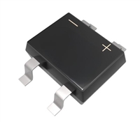 数据手册解读:MB10S引脚说明、电气参数

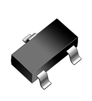 2N7002K资料解读:产品特性和型号推荐
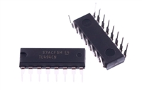 资料解读:TL494CN参数和引脚功能图说明
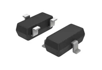 解读BAT54A数据手册:全面解析产品特性与应用


 浙公网安备 33010502006866号 浙ICP备10014259号-119
营业执照ICP证
浙公网安备 33010502006866号 浙ICP备10014259号-119
营业执照ICP证


