
 5秒后页面跳转

| 是否无铅: | 含铅 | 生命周期: | Active |
| 零件包装代码: | SOT-363 | 包装说明: | LEAD FREE, SC-70, SC-88, SOT-363, 6 PIN |
| 针数: | 6 | Reach Compliance Code: | unknown |
| 风险等级: | 5.7 | Is Samacsys: | N |
| 系列: | LVC/LCX/Z | 输入调节: | STANDARD |
| JESD-30 代码: | R-PDSO-G6 | JESD-609代码: | e3 |
| 长度: | 2 mm | 逻辑集成电路类型: | OTHER DECODER/DRIVER |
| 湿度敏感等级: | NOT SPECIFIED | 功能数量: | 1 |
| 端子数量: | 6 | 最高工作温度: | 85 °C |
| 最低工作温度: | -40 °C | 输出特性: | 3-STATE |
| 输出极性: | TRUE | 封装主体材料: | PLASTIC/EPOXY |
| 封装代码: | TSSOP | 封装形状: | RECTANGULAR |
| 封装形式: | SMALL OUTLINE, THIN PROFILE, SHRINK PITCH | 峰值回流温度(摄氏度): | 260 |
| 传播延迟(tpd): | 10.5 ns | 认证状态: | COMMERCIAL |
| 座面最大高度: | 1.1 mm | 最大供电电压 (Vsup): | 5.5 V |
| 最小供电电压 (Vsup): | 1.65 V | 标称供电电压 (Vsup): | 1.8 V |
| 表面贴装: | YES | 技术: | CMOS |
| 温度等级: | INDUSTRIAL | 端子面层: | MATTE TIN |
| 端子形式: | GULL WING | 端子节距: | 0.65 mm |
| 端子位置: | DUAL | 处于峰值回流温度下的最长时间: | 40 |
| 宽度: | 1.25 mm | Base Number Matches: | 1 |
| 型号 | 品牌 | 获取价格 | 描述 | 数据表 |
| NL7SZ18DFT2G | ONSEMI |
获取价格 |
1−of−2 Non−Inverting Demultiplexer with 3−State Deselected Output |

|
| NL7SZ18DFT2G-L22348 | ONSEMI |
获取价格 |
1:2 Digital Demultiplexer Non-Inverting, 3-State |
|
| NL7SZ18MUR2G | ONSEMI |
获取价格 |
1−of−2 Non−Inverting Demultiplexer with 3−State Deselected Output |
|
| NL7SZ19 | ONSEMI |
获取价格 |
1-of-2 Decoder/ Demultiplexer |
|
| NL7SZ19_07 | ONSEMI |
获取价格 |
1−to−2 Decoder/Demultiplexer |
|
| NL7SZ19DFT1 | ONSEMI |
获取价格 |
OTHER DECODER/DRIVER, TRUE OUTPUT, PDSO6, SOT-363, SC-88, SC-70, 6 PIN |
|
| NL7SZ19DFT2 | ONSEMI |
获取价格 |
1-of-2 Decoder/ Demultiplexer |
|
| NL7SZ19DFT2G | ONSEMI |
获取价格 |
1-of-2 Decoder/ Demultiplexer |
|
| NL7SZ19MUR2G | ONSEMI |
获取价格 |
1−to−2 Decoder/Demultiplexer |
|
| NL7SZ57 | ONSEMI |
获取价格 |
Configurable Multifunction Gate |
|
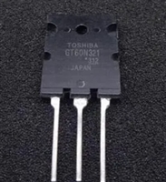 GT60N321资料手册解读:深入了解东芝第四代绝缘栅双极晶体管

 STS5DNE30L资料手册解读:参数分析、特性与应用
 MDU1511资料手册解读:探索这款MOSFET的全面特性
 2SB1260资料手册解读:电气参数、产品特性
工作时间:9:00-21:00
CEO邮箱:ceo@jiepei.com
投诉邮箱:tousu@jiepei.com


 浙公网安备 33010502006866号 浙ICP备10014259号-119
营业执照ICP证
浙公网安备 33010502006866号 浙ICP备10014259号-119
营业执照ICP证


