
| 型号 | 品牌 | 获取价格 | 描述 | 数据表 |
| FOX922BE-40.000MHZ | FOX |
获取价格 |
Oscillator |

|
| FOX922BE-GP | FOX |
获取价格 |
1.8V ~ 3.3V SMD TCXO for GPS Applications |
|
| FOX922BE-GP-16.368MHZ | FOX |
获取价格 |
Oscillator |
|
| FOX922BE-GP-16.369MHZ | FOX |
获取价格 |
Oscillator |
|
| FOX922BE-GP-16.800MHZ | FOX |
获取价格 |
Oscillator |
|
| FOX922BE-GP-24.5535MHZ | FOX |
获取价格 |
Oscillator |
|
| FOX922BE-GP-26.000MHZ | FOX |
获取价格 |
Oscillator |
|
| FOX922BE-GP-33.600MHZ | FOX |
获取价格 |
Oscillator |
|
| FOX922BE-GP-38.400MHZ | FOX |
获取价格 |
Oscillator |
|
| FOX922C-10.000MHZ | FOX |
获取价格 |
Oscillator |
|
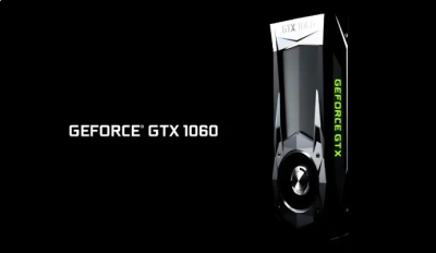 英伟达驱动支持期限敲定:Maxwell/Pascal/Volta架构仅剩最后一年

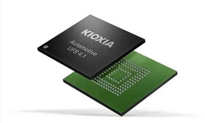 铠侠车用UFS 4.1闪存发布:性能飙升3.7倍,1TB容量改写车载存储格局
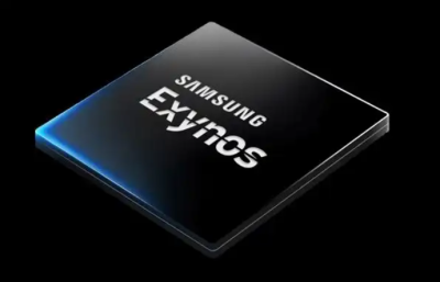 三星抢跑2纳米时代!Exynos 2600芯片或成Galaxy S26杀手锏
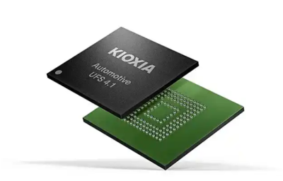 铠侠车规级UFS 4.1震撼发布:随机写入速度飙升至3.7倍
工作时间:9:00-21:00
CEO邮箱:ceo@jiepei.com
投诉邮箱:tousu@jiepei.com


 浙公网安备 33010502006866号 浙ICP备10014259号-119
营业执照ICP证
浙公网安备 33010502006866号 浙ICP备10014259号-119
营业执照ICP证


