DRV8300
SLVSFG5 – SEPTEMBER 2020
www.ti.com
6 Pin Configuration and Functions
INLA
INLB
1
2
3
4
5
6
18 SHA
17
16
BSTB
GHB
DRV8300
INLC
GVDD
15 SHB
PowerPAD
14
MODE
GND
BSTC
13
GHC
Figure 6-1. DRV8300D, DRV8300N RGE Package 24-Pin VQFN With Exposed Thermal Pad Top View
Table 6-1. Pin Functions—24-Pin DRV8300 Devices
PIN
TYPE(1)
DESCRIPTION
NAME
BSTA
BSTB
BSTC
DT
NO.
20
17
14
21
19
16
13
11
10
9
O
O
O
I
Bootstrap output pin. Connect capacitor between BSTA and SHA
Bootstrap output pin. Connect capacitor between BSTB and SHB
Bootstrap output pin. Connect capacitor between BSTC and SHC
Deadtime input pin. Connect resistor to ground for variable deadtime, fixed deadtime when left it floating
High-side gate driver output. Connect to the gate of the high-side power MOSFET.
High-side gate driver output. Connect to the gate of the high-side power MOSFET.
High-side gate driver output. Connect to the gate of the high-side power MOSFET.
Low-side gate driver output. Connect to the gate of the low-side power MOSFET.
Low-side gate driver output. Connect to the gate of the low-side power MOSFET.
Low-side gate driver output. Connect to the gate of the low-side power MOSFET.
High-side gate driver control input. This pin controls the output of the high-side gate driver.
High-side gate driver control input. This pin controls the output of the high-side gate driver.
High-side gate driver control input. This pin controls the output of the high-side gate driver.
Low-side gate driver control input. This pin controls the output of the low-side gate driver.
Low-side gate driver control input. This pin controls the output of the low-side gate driver.
Low-side gate driver control input. This pin controls the output of the low-side gate driver.
GHA
GHB
GHC
GLA
O
O
O
O
O
O
I
GLB
GLC
INHA
INHB
INHC
INLA
INLB
INLC
22
23
24
1
I
I
I
2
I
3
I
Mode Input controls polarity of GLx compared to INLx inputs.
MODE
5
I
Mode pin floating: GLx output polarity same(Non-Inverted) as INLx input
Mode pin to GVDD: GLx output polarity inverted compared to INLx input
NC
7, 8
6
NC
No internal connection. This pin can be left floating or connected to system ground.
Device ground.
GND
SHA
SHB
SHC
PWR
18
15
12
I
I
I
High-side source sense input. Connect to the high-side power MOSFET source.
High-side source sense input. Connect to the high-side power MOSFET source.
High-side source sense input. Connect to the high-side power MOSFET source.
Gate driver power supply input. Connect a X5R or X7R, GVDD-rated ceramic and greater then or equal to 10-uF local capacitance
between the GVDD and GND pins.
GVDD
4
PWR
(1) PWR = power, I = input, O = output, NC = no connection
Copyright © 2020 Texas Instruments Incorporated
4
Submit Document Feedback
Product Folder Links: DRV8300


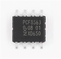
 pcf8563芯片功能说明、参数分析、引脚说明

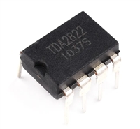
 TDA2822资料手册:引脚说明、参数分析

 TJA1050资料数据分析、引脚说明、应用示例介绍

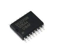
 DS3231时钟芯片:参数分析、引脚说明、应用示例介绍
