
| 型号 | 品牌 | 获取价格 | 描述 | 数据表 |
| DP7419 | NIDEC |
获取价格 |
Dual Digital Potentiometers |

|
| DP74H4B | FREQUENCYDEVICES |
获取价格 |
16 Pin DIP 4-Pole Filters |
|
| DP74H4B-250KHZ | ETC |
获取价格 |
16 Pin DIP 4-Pole Filters |
|
| DP74H4B-33.3KHZ | ETC |
获取价格 |
16 Pin DIP 4-Pole Filters |
|
| DP74H4B-849HZ | ETC |
获取价格 |
16 Pin DIP 4-Pole Filters |
|
| DP74H4L | FREQUENCYDEVICES |
获取价格 |
16 Pin DIP 4-Pole Filters |
|
| DP74H4L-250KHZ | ETC |
获取价格 |
16 Pin DIP 4-Pole Filters |
|
| DP74H4L-33.3KHZ | ETC |
获取价格 |
16 Pin DIP 4-Pole Filters |
|
| DP74H4L-849HZ | ETC |
获取价格 |
16 Pin DIP 4-Pole Filters |
|
| DP74L4B | FREQUENCYDEVICES |
获取价格 |
16 Pin DIP 4-Pole Filters |
|
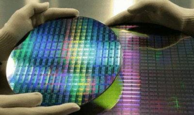 SEMI报告:HBM占比达25%或将引爆硅晶圆产能危机

 AI新贵天价收购计划曝光!Perplexity拟345亿美元鲸吞谷歌Chrome浏览器
 华为UCM技术突破HBM封锁 国产AI推理迎来里程碑式创新
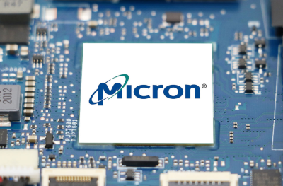 美光战略大调整:全球停止移动NAND开发专注更高利润领域
工作时间:9:00-21:00
CEO邮箱:ceo@jiepei.com
投诉邮箱:tousu@jiepei.com


 浙公网安备 33010502006866号 浙ICP备10014259号-119
营业执照ICP证
浙公网安备 33010502006866号 浙ICP备10014259号-119
营业执照ICP证


