
| 型号 | 品牌 | 获取价格 | 描述 | 数据表 |
| CY7C1380A-167AC | CYPRESS |
获取价格 |
Cache SRAM, 512KX36, 3.4ns, CMOS, PQFP100, 14 X 20 MM, 1.40 MM HEIGHT, PLASTIC, TQFP-100 |

|
| CY7C1380A-167BGC | CYPRESS |
获取价格 |
Cache SRAM, 512KX36, 3.4ns, CMOS, PBGA119, 14 X 22 MM, 2.40 MM HEIGHT, FBGA-119 |
|
| CY7C1380AV25-100BGC | CYPRESS |
获取价格 |
Cache SRAM, 512KX36, 5ns, CMOS, PBGA119, 14 X 22 MM, 2.40 MM HEIGHT, FBGA-119 |
|
| CY7C1380AV25-133AC | CYPRESS |
获取价格 |
Cache SRAM, 512KX36, 4.2ns, CMOS, PQFP100, 14 X 20 MM, 1.40 MM HEIGHT, PLASTIC, TQFP-100 |
|
| CY7C1380AV25-150AC | CYPRESS |
获取价格 |
Cache SRAM, 512KX36, 3.8ns, CMOS, PQFP100, 14 X 20 MM, 1.40 MM HEIGHT, PLASTIC, TQFP-100 |
|
| CY7C1380AV25-150BGC | CYPRESS |
获取价格 |
Cache SRAM, 512KX36, 3.8ns, CMOS, PBGA119, 14 X 22 MM, 2.40 MM HEIGHT, FBGA-119 |
|
| CY7C1380AV25-167AC | CYPRESS |
获取价格 |
Cache SRAM, 512KX36, 3.4ns, CMOS, PQFP100, 14 X 20 MM, 1.40 MM HEIGHT, PLASTIC, TQFP-100 |
|
| CY7C1380B | CYPRESS |
获取价格 |
512K x 36/1M x 18 Pipelined SRAM |
|
| CY7C1380B-133AC | CYPRESS |
获取价格 |
512K x 36/1M x 18 Pipelined SRAM |
|
| CY7C1380B-133AI | CYPRESS |
获取价格 |
512K x 36/1M x 18 Pipelined SRAM |
|
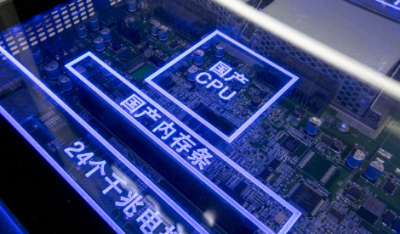 国产AI算力崛起!阿里百度用自研芯片开启AI新时代

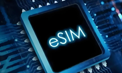 中国三大运营商全面布局eSIM业务 用户何时能用上?
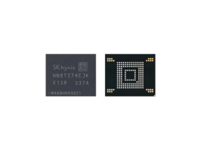 ZUFS 4.1问世!SK海力士新一代闪存如何改写移动端性能格局?
 博通斩获OpenAI百亿订单,能否撼动英伟达AI芯片霸主地位
工作时间:9:00-21:00
CEO邮箱:ceo@jiepei.com
投诉邮箱:tousu@jiepei.com


 浙公网安备 33010502006866号 浙ICP备10014259号-119
营业执照ICP证
浙公网安备 33010502006866号 浙ICP备10014259号-119
营业执照ICP证


