
 5秒后页面跳转

| 是否Rohs认证: | 不符合 | 生命周期: | Obsolete |
| 零件包装代码: | TSSOP | 包装说明: | TSSOP-48 |
| 针数: | 48 | Reach Compliance Code: | compliant |
| ECCN代码: | EAR99 | HTS代码: | 8542.39.00.01 |
| 风险等级: | 5.88 | JESD-30 代码: | R-PDSO-G48 |
| JESD-609代码: | e0 | 长度: | 12.5 mm |
| 端子数量: | 48 | 最高工作温度: | 70 °C |
| 最低工作温度: | 最大输出时钟频率: | 133.33 MHz | |
| 封装主体材料: | PLASTIC/EPOXY | 封装代码: | TSSOP |
| 封装等效代码: | TSSOP48,.3,20 | 封装形状: | RECTANGULAR |
| 封装形式: | SMALL OUTLINE, THIN PROFILE, SHRINK PITCH | 峰值回流温度(摄氏度): | NOT SPECIFIED |
| 电源: | 3.3 V | 主时钟/晶体标称频率: | 33.33 MHz |
| 认证状态: | Not Qualified | 座面最大高度: | 1.2 mm |
| 子类别: | Clock Generators | 最大压摆率: | 30 mA |
| 最大供电电压: | 3.465 V | 最小供电电压: | 3.135 V |
| 标称供电电压: | 3.3 V | 表面贴装: | YES |
| 技术: | CMOS | 温度等级: | COMMERCIAL |
| 端子面层: | Tin/Lead (Sn/Pb) | 端子形式: | GULL WING |
| 端子节距: | 0.5 mm | 端子位置: | DUAL |
| 处于峰值回流温度下的最长时间: | NOT SPECIFIED | 宽度: | 6.1 mm |
| uPs/uCs/外围集成电路类型: | CLOCK GENERATOR, PROCESSOR SPECIFIC | Base Number Matches: | 1 |
| 型号 | 品牌 | 描述 | 获取价格 | 数据表 |
| C9531 | CYPRESS | PCIX I/O System Clock Generator with EMI Control Features |
获取价格 |

|
| C9531_04 | CYPRESS | PCIX I/O System Clock Generator with EMI Control Features |
获取价格 |
|
| C9531AT | CYPRESS | Processor Specific Clock Generator, CMOS, PDSO28, TSSOP-28 |
获取价格 |
|
| C9531AY | CYPRESS | Processor Specific Clock Generator, CMOS, PDSO28, SSOP-28 |
获取价格 |
|
| C9531CT | ETC | CPU SYSTEM CLOCK GENERATOR|TSSOP|28PIN|PLASTIC |
获取价格 |
|
| C9531CY | ETC | CPU SYSTEM CLOCK GENERATOR|SSOP|28PIN|PLASTIC |
获取价格 |
|
 ADXL345传感器工作原理、参数分析、引脚说明

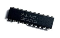 一文带你了解,DAC0832工作原理、输出电压范围、分辨率等参数
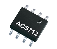 ACS712电流检测使用指南及资料手册参数分析
 TLP521资料手册解读:参数分析、引脚说明、典型电路
工作时间:9:00-21:00
CEO邮箱:ceo@jiepei.com
投诉邮箱:tousu@jiepei.com


 浙公网安备 33010502006866号 浙ICP备10014259号-119
营业执照ICP证
浙公网安备 33010502006866号 浙ICP备10014259号-119
营业执照ICP证


