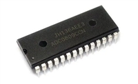
ATF1508AS/Z
All ATF1508s also have an optional power down mode. In
this mode, current drops to below 10 mA. When the power
down option is selected, either PD1 or PD2 pins (or both)
can be used to power down the part. The power down
option is selected in the design source file. When enabled,
the device goes into power down when either PD1 or PD2
is high. In the power down mode, all internal logic signals
are latched and held, as are any enabled outputs.
uncertainty of how VCC actually rises in the system, the fol-
lowing conditions are required:
1. The VCC rise must be monotonic,
2. After reset occurs, all input and feedback setup times
must be met before driving the clock pin high, and,
3. The clock must remain stable during TPR
.
Security Fuse Usage
All pin transitions are ignored until the PD pin is brought
low. When the power down feature is enabled, the PD1 or
PD2 pin cannot be used as a logic input or output. How-
ever, the pin’s macrocell may still be used to generate bur-
ied foldback and cascade logic signals.
A single fuse is provided to prevent unauthorized copying
of the ATF1508AS fuse patterns. Once programmed, fuse
verify is inhibited. However, User Signature and device ID
remains accessible.
All Power-Down AC Characteristic parameters are com-
puted from external input or I/O pins, with Reduced Power
Bit turned on. For macrocells in reduced-power mode
(Reduced power bit turned on), the reduced power adder,
tRPA, must be added to the AC parameters, which include
Programming
ATF1508AS devices are In-System Programmable (ISP)
devices utilizing the 4-pin JTAG protocol. This capability
eliminates package handling normally required for program
and facilitates rapid design iterations and field changes.
the data paths tLAD, tLAC, tIC, tACL, tACH and tSEXP
.
Each output also has individual slew rate control. This may
be used to reduce system noise by slowing down outputs
that do not need to operate at maximum speed. Outputs
default to slow switching, and may be specified as fast
switching in the design file.
Atmel provides ISP hardware and software to allow pro-
gramming of the ATF1508AS via the PC. ISP is perfomed
by using either a download cable, or a comparable board
tester or a simple microprocessor interface.
To facilitate ISP programming by the Automated Test
Equipment (ATE) vendors, Serial Vector Format (SVF)
files can be created by Atmel provided Software utilities.
Design Software Support
ATF1508AS designs are supported by several third party
tools. Automated fitters allow logic synthesis using a variety
of high level description languages and formats.
ATF1508AS devices can also be programmed using stan-
dard 3rd party programmers. With 3rd party programmer
the JTAG ISP port can be disabled thereby allowing 4 addi-
tional I/O pins to be used for logic.
Power Up Reset
Contact your local Atmel representatives or Atmel PLD
applications for details.
The ATF1508AS has a power-up reset option at two differ-
ent voltage trip levels when the device is being powered
down. Within the fitter, or during a conversion, if the
“power-reset” option is turned “on” ( which is the default
option), the trip levels during power up or power down is at
2.8V. The user can change this default option from “on” to
“off” (within the fitter or specify it as a switch during conver-
sion). When this is done, the voltage trip level during
power-down changes from 2.8V to 0.7V. This is to ensure a
robust operating environment.
ISP Programming Protection
The ATF1508AS has a special feature which locks the
device and prevents the inputs and I/O from driving if the
programming process is interrupted due to any reason. The
inputs and I/O default to high-Z state during such a condi-
tion. In addition the pin keeper option preserves the former
state during device programming.
All ATF1508AS devices are initially shipped in the erased
state thereby making them ready to use for ISP.
The registers in the ATF1508AS are designed to reset dur-
ing power up. At a point delayed slightly from VCC crossing
VRST, all registers will be reset to the low state. The output
state will depend on the polarity of the buffer.
Note:
For more information refer to the “Desigining for In-Sys-
tem Programmability with Atmel CPLDs” application
note.
This feature is critical for state machine initialization. How-
ever, due to the asynchronous nature of reset and the
7


 SI2301 N沟道MOSFET:资料手册参数分析

 ADC0809逐次逼近寄存器型模数转换器:资料手册参数分析

 AD9361捷变收发器:全面参数解析与关键特性概览

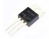
 IRF3205功率MOSFET:资料手册参数分析
