3UHOLPLQDU\ꢀLQIRUPDWLRQ
$6ꢁꢂ)ꢃꢃꢁ
®
)XQFWLRQDOꢀGHVFULSWLRQ
The AS29F002 is a 2 megabit, 5 volt only Flash memory organized as 256K bytes of 8 bits each. For flexible erase and program capability, the 2
megabits of data is divided into 7 sectors: one 16K byte, two 8K byte, one 32K byte, and three 64K bytes. The data appears on DQ0–DQ7. The
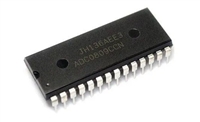
AS29F002 is offered in JEDEC standard 40-pin TSOP, 32-pin PLCC, 32-pin TSOP, and 32-pin PDIP packages. This device is designed to be
programmed and erased in-sytem with a single 5.0V VCC supply. The device can also be reprogrammed in standard EPROM programmers.
The AS29F002 offers access times of 55/ 70/ 90/ 120 ns, allowing 0-wait state operation of high speed microprocessors. To eliminate bus contention
the device has separate chip enable (CE), write enable (WE), and output enable (OE) controls.
The AS29F002 is fully compatible with the JEDEC single power supply Flash standard. Write commands to the command register using standard
microprocessor write timings. An internal state-machine uses register contents to control the erase and programming circuitry. Write cycles also
internally latch addresses and data needed for the programming and erase operations. Read data from the device in the same manner as other Flash or
EPROM devices. Use the program command sequence to invoke the automated on-chip programming algorithm that automatically times the
program pulse widths and verifies proper cell margin. Use the erase command sequence to invoke the automated on-chip erase algorithm that
preprograms the sector if it is not already programmed before executing the erase operation, times the erase pulse widths, and verifies proper cell
margin.
Boot sector architecture enables the device to boot from either the top (AS29F002T) or bottom (AS29F002B) sector. Sector erase architecture allows
specified sectors of memory to be erased and reprogrammed without altering data in other sectors. A sector typically erases and verifies within 1.6
seconds. Hardware sector protection disables both program and erase operations in all or any combination of the seven sectors. The device provides
background erase with Erase Suspend, which puts erase operations on hold to read data from a sector that is not being erased. The chip erase
command will automatically erase all unprotected sectors.
A factory shipped AS29F002 is fully erased (all bits = 1). The programming operation sets bits to 0. Data is programmed into the array one byte at a
time in any sequence and across sector boundaries. A sector must be erased to change bits from 0 to 1. Erase returns all bytes in a sector to the erased
state (all bits = 1). Each sector is erased individually with no effect on other sectors.
The device features single 5.0V power supply operation for both read and write functions. Internally generated and regulated voltages are provided
for the program and erase operations. A low VCC detector automatically inhibits write operations during power transtitions. DATA polling of DQ7 or
toggle bit (DQ6) may be used to detect end of program or erase operations. The device automatically resets to the read mode after program/ erase
operations are completed.
The AS29F002 resists accidental erasure or spurious programming signals resulting from power transitions. Control register architecture permits
alteration of memory contents only after successful completion of specific command sequences. During power up, the device is set to read mode
with all program/ erase commands disabled when VCC is less than VLKO (lockout voltage). The command registers are not affected by noise pulses of
less than 5 ns on OE, CE, or WE. CE and WE must be logical zero and OE a logical one to initiate write commands.
When the device’s hardware RESET pin is driven low, any program/ erase operation in progress will be terminated and the internal state machine will
be reset to read mode. If the RESET pin is tied to the system reset circuitry and a system reset occurs during an automated on-chip program/ erase
algorithm, data in address locations being operated on will become corrupted and require rewriting. Resetting the device enables the system’s
microprocessor to read boot-up firmware from the Flash memory.
The AS29F002 uses Fowler-Nordheim tunnelling to electrically erase all bits within a sector simultaneously. Bytes are programmed one at a time
using EPROM programming mechanism of hot electron injection.
/RJLFꢀEORFNꢀGLDJUDP
Sector protect
DQ0–DQ7
switches
VCC
V
RESET
SS
Erase voltage
generator
Input/ output
buffers
Program/ erase
control
WE
Program voltage
generator
Command
register
STB
Chip enable
Output enable
Logic
Data latch
CE
OE
Y decoder
Y gating
STB
VCC detector
Timer
X decoder
Cell matrix
A0–A17
ꢄꢅꢃ
$//,$1&(ꢀ6(0,&21'8&725


 SI2301 N沟道MOSFET:资料手册参数分析

 ADC0809逐次逼近寄存器型模数转换器:资料手册参数分析

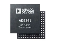
 AD9361捷变收发器:全面参数解析与关键特性概览

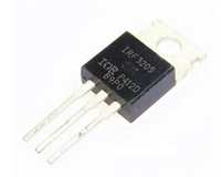
 IRF3205功率MOSFET:资料手册参数分析
