ADSP-21362/ADSP-21363/ADSP-21364/ADSP-21365/ADSP-21366
processing, and are commonly used in digital filters and Fourier
transforms. The two DAGs contain sufficient registers to allow
the creation of up to 32 circular buffers (16 primary register sets,
16 secondary). The DAGs automatically handle address pointer
wraparound, reduce overhead, increase performance, and sim-
plify implementation. Circular buffers can start and end at any
memory location.
Data Register File
Each processing element contains a general-purpose data regis-
ter file. The register files transfer data between the computation
units and the data buses, and store intermediate results. These
10-port, 32-register (16 primary, 16 secondary) files, combined
with the ADSP-2136x enhanced Harvard architecture, allow
unconstrained data flow between computation units and inter-
nal memory. The registers in PEX are referred to as R0–R15 and
in PEY as S0–S15.
Flexible Instruction Set
The 48-bit instruction word accommodates a variety of parallel
operations for concise programming. For example, the
processor can conditionally execute a multiply, an add, and a
subtract in both processing elements while branching and fetch-
ing up to four 32-bit values from memory—all in a single
instruction.
Context Switch
Many of the processor’s registers have secondary registers that
can be activated during interrupt servicing for a fast context
switch. The data registers in the register file, the DAG registers,
and the multiplier result register all have secondary registers.
The primary registers are active at reset, while the secondary
registers are activated by control bits in a mode control register.
On-Chip Memory
The processor contains 3M bits of internal SRAM and 4M bits
of internal ROM. Each block can be configured for different
combinations of code and data storage (see Table 3). Each
memory block supports single-cycle, independent accesses by
the core processor and I/O processor. The processor’s memory
architecture, in combination with its separate on-chip buses,
allows two data transfers from the core and one from the I/O
processor, in a single cycle.
Universal Registers
The universal registers are general purpose registers. The
USTAT (4) registers allow easy bit manipulations (Set, Clear,
Toggle, Test, XOR) for all system registers (control/status) of
the core.
The data bus exchange register (PX) permits data to be passed
between the 64-bit PM data bus and the 64-bit DM data bus, or
between the 40-bit register file and the PM/DM data bus. These
registers contain hardware to handle the data width difference.
The SRAM can be configured as a maximum of 96K words of
32-bit data, 192K words of 16-bit data, 64K words of 48-bit
instructions (or 40-bit data), or combinations of different word
sizes up to 3M bits. All of the memory can be accessed as 16-bit,
32-bit, 48-bit, or 64-bit words. A 16-bit floating-point storage
format is supported that effectively doubles the amount of data
that can be stored on-chip. Conversion between the 32-bit
floating-point and 16-bit floating-point formats is performed in
a single instruction. While each memory block can store combi-
nations of code and data, accesses are most efficient when one
block stores data using the DM bus for transfers, and the other
block stores instructions and data using the PM bus for
transfers.
Timer
A core timer that can generate periodic software interrupts. The
core timer can be configured to use FLAG3 as a timer expired
signal.
Single-Cycle Fetch of Instruction and Four Operands
The processor features an enhanced Harvard architecture in
which the data memory (DM) bus transfers data and the pro-
gram memory (PM) bus transfers both instructions and data
(see Figure 2). With the its separate program and data memory
buses and on-chip instruction cache, the processor can simulta-
neously fetch four operands (two over each data bus) and one
instruction (from the cache), all in a single cycle.
Using the DM bus and PM buses, with one bus dedicated to
each memory block, assures single-cycle execution with two
data transfers. In this case, the instruction must be available in
the cache.
Instruction Cache
On-Chip Memory Bandwidth
The processor includes an on-chip instruction cache that
enables three-bus operation for fetching an instruction and four
data values. The cache is selective—only the instructions whose
fetches conflict with PM bus data accesses are cached. This
cache allows full-speed execution of core looped operations
such as digital filter multiply-accumulates, and FFT butterfly
processing.
The internal memory architecture allows three accesses at the
same time to any of the four blocks, assuming no block con-
flicts. The total bandwidth is gained with DMD and PMD buses
(2 × 64-bits, core CLK) and the IOD bus (32-bit, PCLK).
ROM-Based Security
The processor has a ROM security feature that provides hard-
ware support for securing user software code by preventing
unauthorized reading from the internal code. When using this
feature, the processor does not boot-load any external code, exe-
cuting exclusively from internal ROM. Additionally, the
processor is not freely accessible via the JTAG port. Instead, a
unique 64-bit key, which must be scanned in through the JTAG
Data Address Generators with Zero-Overhead Hardware
Circular Buffer Support
The processor’s two data address generators (DAGs) are used
for indirect addressing and implementing circular data buffers
in hardware. Circular buffers allow efficient programming of
delay lines and other data structures required in digital signal
Rev. J
|
Page 5 of 60
|
July 2013


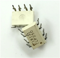
 TLP250光耦合器:资料手册参数分析

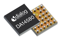
 DA14580 低功耗蓝牙系统级芯片(SoC):资料手册参数分析

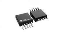
 INA226 高精度电流和功率监控器:资料手册参数分析

 SI2302 N沟道MOSFET:资料手册参数分析
