ADSP-21065L
PIN DESCRIPTIONS
ADSP-21065L pin definitions are listed below. Inputs identified as synchronous (S) must meet timing requirements with respect to
CLKIN (or with respect to TCK for TMS, TDI). Inputs identified as asynchronous (A) can be asserted asynchronously to CLKIN
(or to TCK for TRST).
Unused inputs should be tied or pulled to VDD or GND, except for ADDR23-0, DATA31-0, FLAG11-0, SW, and inputs that have
internal pull-up or pull-down resistors (CPA, ACK, DTxX, DRxX, TCLKx, RCLKx, TMS, and TDI)—these pins can be left float-
ing. These pins have a logic-level hold circuit that prevents the input from floating internally.
I = Input
O = Output
S = Synchronous
A = Asynchronous
P = Power Supply
G = Ground
(O/D) = Open Drain
(A/D) = Active Drive
T = Three-state (when SBTS is asserted, or when the ADSP-2106x is a bus slave)
Pin
Type
Function
ADDR23-0
I/O/T
External Bus Address. The ADSP-21065L outputs addresses for external memory and
peripherals on these pins. In a multiprocessor system the bus master outputs addresses for read/
writes of the IOP registers of the other ADSP-21065L. The ADSP-21065L inputs addresses
when a host processor or multiprocessing bus master is reading or writing its IOP registers.
DATA31-0
I/O/T
I/O/T
External Bus Data. The ADSP-21065L inputs and outputs data and instructions on these
pins. The external data bus transfers 32-bit single-precision floating-point data and 32-bit fixed-
point data over bits 31-0. 16-bit short word data is transferred over bits 15-0 of the bus. Pull-up
resistors on unused DATA pins are not necessary.
MS3-0
Memory Select Lines. These lines are asserted as chip selects for the corresponding banks of
external memory. Internal ADDR25-24 are decoded into MS3-0. The MS3-0 lines are decoded
memory address lines that change at the same time as the other address lines. When no external
memory access is occurring the MS3-0 lines are inactive; they are active, however, when a condi-
tional memory access instruction is executed, whether or not the condition is true. Additionally,
an MS3-0 line which is mapped to SDRAM may be asserted even when no SDRAM access is
active. In a multiprocessor system, the MS3-0 lines are output by the bus master.
RD
WR
SW
I/O/T
I/O/T
I/O/T
Memory Read Strobe. This pin is asserted when the ADSP-21065L reads from external memory
devices or from the IOP register of another ADSP-21065L. External devices (including another
ADSP-21065L) must assert RD to read from the ADSP-21065L’s IOP registers. In a multipro-
cessor system, RD is output by the bus master and is input by another ADSP-21065L.
Memory Write Strobe. This pin is asserted when the ADSP-21065L writes to external memory
devices or to the IOP register of another ADSP-21065L. External devices must assert WR to
write to the ADSP-21065L’s IOP registers. In a multiprocessor system, WR is output by the bus
master and is input by the other ADSP-21065L.
Synchronous Write Select. This signal interfaces the ADSP-21065L to synchronous memory
devices (including another ADSP-21065L). The ADSP-21065L asserts SW to provide an early
indication of an impending write cycle, which can be aborted if WR is not later asserted (e.g., in
a conditional write instruction). In a multiprocessor system, SW is output by the bus master and
is input by the other ADSP-21065L to determine if the multiprocessor access is a read or write.
SW is asserted at the same time as the address output.
ACK
I/O/S
Memory Acknowledge. External devices can deassert ACK to add wait states to an external
memory access. ACK is used by I/O devices, memory controllers, or other peripherals to hold
off completion of an external memory access. The ADSP-21065L deasserts ACK as an output
to add wait states to a synchronous access of its IOP registers. In a multiprocessor system, a
slave ADSP-21065L deasserts the bus master’s ACK input to add wait state(s) to an access of
its IOP registers. The bus master has a keeper latch on its ACK pin that maintains the input at
the level to which it was last driven.
SBTS
I/S
Suspend Bus Three-State. External devices can assert SBTS to place the external bus address,
data, selects, and strobes—but not SDRAM control pins—in a high impedance state for the
following cycle. If the ADSP-21065L attempts to access external memory while SBTS is as-
serted, the processor will halt and the memory access will not finish until SBTS is deasserted.
SBTS should only be used to recover from host processor/ADSP-21065L deadlock.
IRQ2-0
I/A
Interrupt Request Lines. May be either edge-triggered or level-sensitive.
FLAG11-0
I/O/A
Flag Pins. Each is configured via control bits as either an input or an output. As an input, it can
be tested as a condition. As an output, it can be used to signal external peripherals.
REV. C
–7–


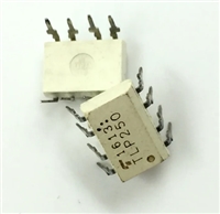
 TLP250光耦合器:资料手册参数分析

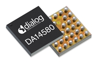
 DA14580 低功耗蓝牙系统级芯片(SoC):资料手册参数分析

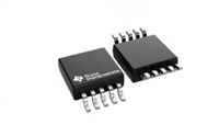
 INA226 高精度电流和功率监控器:资料手册参数分析

 SI2302 N沟道MOSFET:资料手册参数分析
