Data Sheet
AD5592R
Parameter
Min
Typ
Max
Unit1
Test Conditions/Comments
VDD = 3 V (Normal Mode)
1.1
mA
I/O0 to I/O7 are DACs, internal reference,
gain = 1
1
mA
mA
mA
mA
mA
I/O0 to I/O7 are DACs, external reference,
gain = 1
I/O0 to I/O7 are DACs and sampled by the
ADC, internal reference, gain = 1
I/O0 to I/O7 are DACs and sampled by the
ADC, external reference, gain = 1
I/O0 to I/O7 are ADCs, internal reference,
gain = 1
1.1
0.78
0.75
0.5
I/O0 to I/O7 are ADCs, external reference,
gain = 1
0.45
0.45
mA
mA
V
I/O0 to I/O7 are general-purpose outputs
I/O0 to I/O7 are general-purpose inputs
AD5592R-1 only
VLOGIC
ILOGIC
1.8
VDD
3
µA
AD5592R-1 only
1 All specifications expressed in decibels are referred to full-scale input (FSR) and tested with an input signal at 0.5 dB below full scale, unless otherwise noted.
2 Guaranteed by design and characterization; not production tested.
3 DC specifications tested with the outputs unloaded, unless otherwise noted. Linearity calculated using a code range of 8 to 4095. There is an upper dead band of
10 mV when VREF = VDD
.
4 When drawing a load current at either rail, the output voltage headroom with respect to that rail is limited by the 25 Ω typical channel resistance of the output
devices. For example, when sinking 1 mA, the minimum output voltage = 25 Ω × 1 mA = 25 mV (see Figure 33).
TIMING CHARACTERISTICS
Guaranteed by design and characterization, not production tested; all input signals are specified with tR = tF = 5 ns (10% to 90% of VDD
and timed from a voltage level of (VIL + VIH)/2; TA = TMIN to TMAX, unless otherwise noted.
)
Table 3. AD5592R Timing Characteristics
Parameter
2.7 V ≤ VDD < 3 V
3 V ≤ VDD ≤ 5.5 V
Unit
Test Conditions/Comments
t1
33
50
16
16
15
2
20
50
10
10
10
2
ns min
ns min
ns min
ns min
ns min
µs max
ns min
ns min
ns min
ns min
ns min
ns min
ns max
ns min
SCLK cycle time, write operation
SCLK cycle time, read operation
SCLK high time
t2
t3
t4
SCLK low time
SYNC falling edge to SCLK falling edge setup time
SYNC falling edge to SCLK falling edge setup time1
Data setup time
t5
t6
t7
t8
7
5
15
30
60
0
7
5
10
30
60
0
Data hold time
SCLK falling edge to SYNC rising edge
Minimum SYNC high time for register write operations
Minimum SYNC high time for register read operations
SYNC rising edge to next SCLK falling edge
SCLK rising edge to SDO valid
t9
t10
t11
25
250
25
250
RESET low pulse width (not shown in Figure 4)
1 When reading an ADC conversion.
Rev. C | Page 7 of 42


 MAX6675资料手册参数详解、引脚配置说明

 LM258引脚图及功能介绍、主要参数分析

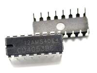
 CD4052资料手册参数详解、引脚配置说明

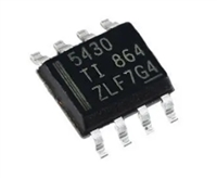
 一文带你了解TPS5430资料手册分析:参数介绍、引脚配置说明
