AD1893
(continued from Page 1)
DEFINITIONS
Dynamic Range
PRODUCT OVERVIEW (Continued)
The ratio of a near full-scale input signal to the integrated noise
in the passband (0 kHz to ≈20 kHz), expressed in decibels (dB).
Dynamic range is measured with a –60 dB input signal and
“60 dB” arithmetically added to the result.
limited to avoid alias distortion on the output signal. The
AD1893 dynamically alters the low-pass filter cutoff frequency
smoothly and slowly, so that real-time variations in the sample
rate ratio are possible without degradation of the audio quality.
Total Harmonic Distortion + Noise
The AD1893 has a pin selectable slow- or fast-settling mode.
This mode determines how quickly the ASRC adapts to a
change in either the input sample clock frequency (FSIN) or the
output sample clock frequency (FSOUT). In the slow-settling
mode, the control loop which computes the ratio between FSIN
and FSOUT settles in approximately 800 ms and begins to reject
jitter above 3 Hz. The slow-settling mode offers the best signal
quality and the greatest jitter rejection. In the fast-settling mode,
the control loop settles in approximately 200 ms and begins to
reject jitter above 12 Hz. The fast-settling mode allows rapid,
real time sample rate changes to be tracked without error, at the
expense of some narrowband noise modulation products on the
output signal.
Total Harmonic Distortion plus Noise (THD+N) is defined as
the ratio of the square root of the sum of the squares of the values
of the harmonics and noise to the rms value of a sinusoidal
input signal. It is usually expressed in percent (%) or decibels.
Interchannel Phase Deviation
Difference in input sampling times between stereo channels,
expressed as a phase difference in degrees between 1 kHz inputs.
Group Delay
Intuitively, the time interval required for a full-level input pulse
to appear at the converter’s output, at full level, expressed in
milliseconds (ms). More precisely, the derivative of radian
phase with respect to radian frequency at a given frequency.
Transport Delay
The AD1893 features short group delay processing. This feature
relates to the depth of the First-In, First-Out (FIFO) memory,
which buffers the input data samples before they are processed
by the FIR convolver. In the AD1893, the group delay is
approximately 700 µs. If the read and write pointers that
manage the FIFO cross (indicating underflow or overflow), the
AD1893 asserts the mute output (MUTE_O) pin HI for 128
output clock cycles. If MUTE_O is connected to the mute input
(MUTE_I) pin, as it normally should be, the serial output will
be muted (i.e., all bits zero) during this transient event.
The time interval between when an impulse is applied to the
converter’s input and when the output starts to be affected by
this impulse, expressed in milliseconds (ms). Transport delay is
independent of frequency.
The AD1893 includes an on-chip oscillator that only requires
the user provide an external crystal. By removing the need for
an external oscillator, the AD1893 lowers the total cost of own-
ership to the end user. The AD1893 also includes a power-
down mode, which is invoked with the PWRDWN pin.
Asserting this control signal HI will place the AD1893 into a
very low power dissipation in active and standby condition.
The AD1893 is fabricated in a 0.8 µm single poly, double metal
CMOS process and are packaged in a 0.6" wide 28-lead plastic
DIP and a 10 mm by 10 mm body size 44-lead LQFP. The
AD1893 operates from a +3 V to +5 V power supply over the
temperature range of 0°C to +70°C.
REV. A
–4–


 MAX6675资料手册参数详解、引脚配置说明

 LM258引脚图及功能介绍、主要参数分析

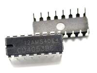
 CD4052资料手册参数详解、引脚配置说明

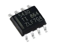
 一文带你了解TPS5430资料手册分析:参数介绍、引脚配置说明
