A29L160A Series
Absolute Maximum Ratings*
*Comments
Stresses above those listed under "Absolute Maximum
Ratings" may cause permanent damage to this device.
These are stress ratings only. Functional operation of
this device at these or any other conditions above
those indicated in the operational sections of these
specification is not implied or intended. Exposure to
the absolute maximum rating conditions for extended periods
may affect device reliability.
Storage Temperature Plastic Packages. . . -65°C to + 150°C
Ambient Temperature with Power Applied. -55°C to + 125°C
Voltage with Respect to Ground
VCC (Note 1) . . . . . . . . . . . . . . . . . . . . ……. . -0.5V to +4.0V
A9,
&
(Note 2) . . . . . . . . . . . …. -0.5 to +12.5V
RESET
OE
All other pins (Note 1) . . . . . . . . . . …. . -0.5V to VCC + 0.5V
Output Short Circuit Current (Note 3) . . . . . . . …. . 200mA
Notes:
Operating Ranges
1. Minimum DC voltage on input or I/O pins is -0.5V. During
voltage transitions, input or I/O pins may undershoot VSS
to -2.0V for periods of up to 20ns. Maximum DC voltage
on input and I/O pins is VCC +0.5V. During voltage
transitions, input or I/O pins may overshoot to VCC +2.0V
for periods up to 20ns.
Commercial (C) Devices
Ambient Temperature (TA) . . . . . . . . . . . ….. . . 0°C to +70°C
Extended Range Devices
Ambient Temperature (TA)
For –I series. . . . . . . . . . . . . . . . . . . . . . . . . . -25°C to +85°C
For –U series . . . . . . . . . . . . . . . . . . . . . . . . . -40°C to +85°C
2. Minimum DC input voltage on A9,
and
is
-
OE
RESET
and
0.5V. During voltage transitions, A9,
OE
RESET
may overshoot VSS to -2.0V for periods of up to 20ns.
Maximum DC input voltage on A9 is +12.5V which may
overshoot to 14.0V for periods up to 20ns.
VCC Supply Voltages
VCC for all devices . . . . . . . . . . . . . . . . . …...+3.0V to +3.6V
Operating ranges define those limits between which the
functionally of the device is guaranteed.
3. No more than one output is shorted at a time. Duration of
the short circuit should not be greater than one second.
Device Bus Operations
execute the command. The contents of the register serve as
inputs to the internal state machine. The state machine
outputs dictate the function of the device. The appropriate
device bus operations table lists the inputs and control levels
required, and the resulting output. The following subsections
describe each of these operations in further detail.
This section describes the requirements and use of the
device bus operations, which are initiated through the
internal command register. The command register itself does
not occupy any addressable memory location. The register is
composed of latches that store the commands, along with
the address and data information needed to
Table 1. A29L160A Device Bus Operations
Operation
A0 – A19
(Note 1)
I/O0 - I/O7
I/O8 - I/O15
=VIH
WE
CE
OE
RESET
=VIL
BYTE
BYTE
I/O8~I/O4=High-Z
Read
Write
CMOS Standby
Output Disable
Hardware Reset
L
L
H
H
AIN
DOUT
DOUT
I/O15=A-1
High-Z
High-Z
L
H
X
H
X
L
X
H
X
H
AIN
X
DIN
DIN
High-Z
High-Z
High-Z
High-Z
High-Z
High-Z
VCC ± 0.3 V
VCC ± 0.3 V
L
X
H
L
X
X
High-Z
High-Z
Sector Protect
(See Note 2)
Sector Unprotect
(See Note 2)
Temporary Sector
Unprotect
Sector Address,
A6=L, A1=H, A0=L
Sector Address,
A6=H, A1=H, A0=L
L
L
X
H
H
X
L
L
X
VID
VID
VID
DIN
DIN
DIN
X
X
X
X
X
AIN
DIN
Legend:
L = Logic Low = VIL, H = Logic High = VIH, VID = 12.0 ± 0.5V, X = Don't Care, DIN = Data In, DOUT = Data Out, AIN = Address In
Notes:
1. Addresses are A19:A0 in word mode (
2. See the “Sector Protection/Unprotection” section and Temporary Sector Unprotect for more information.
=VIH), A19: A in byte mode (
=VIL).
BYTE
BYTE
-1
(May, 2005, Version 0.1)
5
AMIC Technology, Corp.


 SI2301 N沟道MOSFET:资料手册参数分析

 ADC0809逐次逼近寄存器型模数转换器:资料手册参数分析

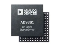
 AD9361捷变收发器:全面参数解析与关键特性概览

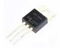
 IRF3205功率MOSFET:资料手册参数分析
