Integrated
Circuit
Systems, Inc.
ICS9LPRS545
Datasheet
Absolute Maximum Ratings - DC Parameters
PARAMETER
SYMBOL
VDDxxx
VDDxxx_IO
VIH
CONDITIONS
Supply Voltage
MIN
MAX
4.6
UNITS Notes
Maximum Supply Voltage
Maximum Supply Voltage
Maximum Input Voltage
V
V
V
7
7
Low-Voltage Differential I/O Supply
3.3V Inputs
3.8
4.6
4,5,7
Minimum Input Voltage
Storage Temperature
Input ESD protection
VIL
Ts
Any Input
GND - 0.5
-65
V
°C
4,7
4,7
6,7
-
150
ESD prot
Human Body Model
2000
V
1Guaranteed by design and characterization, not 100% tested in production.
2 Operation under these conditions is neither implied, nor guaranteed.
3 Maximum input voltage is not to exceed VDD
AC Electrical Characteristics - Low Power Differential Outputs
PARAMETER
Rising Edge Slew Rate
Falling Edge Slew Rate
Slew Rate Variation
Differential Voltage Swing
Crossing Point Voltage
Crossing Point Variation
Maximum Output Voltage
Minimum Output Voltage
Duty Cycle
SYMBOL
tSLR
CONDITIONS
Averaging on
MIN
2.5
MAX
4
UNITS NOTES
V/ns
V/ns
%
2, 3
2, 3
1, 10
2
tFLR
Averaging on
2.5
4
tSLVAR
Averaging on
20
VSWING
VXABS
Averaging off
300
300
mV
mV
mV
mV
mV
%
Averaging off
550
140
1,4,5
1,4,9
1,7
VXABSVAR
VHIGH
Averaging off
Averaging off
1150
VLOW
Averaging off
-300
45
1,8
DCYC
Averaging on
55
100
150
3000
2
CPU[1:0] Skew
CPUSKEW10
CPUSKEW20
SRCSKEW
Differential Measurement
Differential Measurement
Differential Measurement
ps
1
CPU[2_ITP:0] Skew
SRC[10:0] Skew
ps
1
ps
1,6,11
NOTES on DIF Output AC Specs: (unless otherwise noted, guaranteed by design and characterization, not 100% tested in production).
1Measurement taken for single ended waveform on a component test board (not in system)
2 Measurement taken from differential waveform on a component test board. (not in system)
3 Slew rate emastured through V_swing voltage range centered about differential zero
4 Vcross is defined at the voltage where Clock = Clock#, measured on a component test board (not in system)
5 Only applies to the differential rising edge (Clock rising, Clock# falling)
6 Total distributed intentional SRC to SRC skew. PCIE Gen2 outputs (SRC3, 4, 6 and 7) will have 0 nominal skew. Maximum allowable interpair skew is 150 ps.
7 The max voltage including overshoot.
8 The min voltage including undershoot.
9 The total variation of all Vcross measurements in any particular system. Note this is a subset of V_cross min/mas (V_Cross absolute) allowed. The intent is to limit Vcross
10 Matching applies to rising edge rate for Clock and falling edge rate for Clock#. It is measured using a +/-75mV window centered on the average cross point where Clock rising
11 For PCIe Gen2 compliant devices, SRC 3, 4, 6, and 7 will have 0 ps nominal skew.
Electrical Characteristics - PCICLK/PCICLK_F
PARAMETER
SYMBOL
CONDITIONS
see Tperiod min-max values
33.33MHz output no spread
33.33MHz output spread
33.33MHz output no spread
33.33MHz output nominal/spread
IOH = -1 mA
MIN
MAX
UNITS NOTES
Long Accuracy
ppm
-100
100
ppm
ns
ns
ns
ns
V
1,2
2
29.99700 30.00300
30.08421 30.23459
29.49700 30.50300
29.56617 30.58421
2.4
Clock period
Tperiod
Tabs
2
2
Absolute min/max period
2
Output High Voltage
Output Low Voltage
VOH
VOL
1
IOL = 1 mA
0.55
V
mA
mA
mA
mA
V/ns
V/ns
ps
1
1
1
1
1
1
1
2
2
2
2
V
OH @MIN = 1.0 V
VOH@MAX = 3.135 V
OL @ MIN = 1.95 V
-33
-33
30
Output High Current
Output Low Current
IOH
IOL
V
VOL @ MAX = 0.4 V
Measured from 0.8 to 2.0 V
Measured from 2.0 to 0.8 V
VT = 1.5 V
38
Rising Edge Slew Rate
Falling Edge Slew Rate
Pin to Pin Skew
tSLR
tFLR
1
1
4
4
tskew
tskew
dt1
250
200
55
Intential PCI to PCI delay
Duty Cycle
VT = 1.5 V
100
45
ps
VT = 1.5 V
%
Jitter, Cycle to cycle
tjcyc-cyc
VT = 1.5 V
500
ps
1479A—07/28/09
5


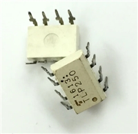
 TLP250光耦合器:资料手册参数分析

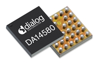
 DA14580 低功耗蓝牙系统级芯片(SoC):资料手册参数分析

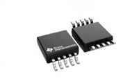
 INA226 高精度电流和功率监控器:资料手册参数分析

 SI2302 N沟道MOSFET:资料手册参数分析
