Integrated
Circuit
Systems, Inc.
ICS9LPRS535
Datasheet
SSOP/TSSOP Pin Description
PIN #
PIN NAME
TYPE
DESCRIPTION
3.3V PCI clock output or CR#_A input. Default is PCI0. To configure this pin as CR#_A, the PCI output must first be disabled in
Byte 2, bit 0.
1
2
3
PCI0/CR#_A
I/O
Byte 5, bit 7: 0 = PCI0 enabled (default), 1= CR#_A enabled.
Byte 5, bit 6: 0 = CR#_A controls SRC0 (default), 1= CR#_A# controls SRC2.
VDDPCI
PWR Power supply for PCI clocks, nominal 3.3V
3.3V PCI clock output / SRC5 enable strap. On powerup, the logic value on this pin determines if SRC5 or
CPU_STOP#/PCI_STOP# is enabled. The latched value controls the pin function as follows
0 = PCI_STOP#/CPU_STOP#
PCI4/SRC5_EN
I/O
1 = SRC5/SRC5#
Free running PCI clock output and ITP/SRC8 enable strap. This output is not affected by the state of the PCI_STOP# pin. On
powerup, the state of this pin determines whether pins 38 and 39 are an ITP or SRC pair.
0 =SRC8/SRC8#
4
PCI_F5/ITP_EN
I/O
1 = ITP/ITP#
5
6
GNDPCI
VDD48
PWR Ground pin for the PCI outputs
PWR Power pin for the 48MHz output.3.3V
3.3V tolerant input for CPU frequency selection. Refer to input electrical characteristics for Vil_FS and Vih_FS values. / Fixed
48MHz USB clock output. 3.3V.
7
USB_48MHz/FSLA
I/O
8
9
GND48
PWR Ground pin for the 48MHz outputs
VDD96_IO
PWR Power pin for the DOT96 clocks, nominal 1.05V to 3.3V.
True clock of push-pull SRC or DOT96 with integrated series resistor. No 50 ohm pull down needed. Default is SRCT0. After
powerup, this pin function may be changed to DOT96T via SMBus Byte 1, bit 7 as follows:
0= SRC0T
10 DOT96T_LPR/SRCT0_LPR
11 DOT96C_LPR/SRCC0_LPR
OUT
1=DOT96T
Complementary clock of push-pull SRC or DOT96 with integrated series resistor. No 50 ohm pull down needed. Default is
SRC0C. After powerup, this pin function may be changed to DOT96C via SMBus Byte 1, bit 7 as follows:
0= SRC0C
OUT
1=DOT96C
12 GND
13 VDD
14 SE1
15 GND
PWR Ground pin.
PWR Power supply, nominal 3.3V
OUT CK505 Singled Ended Output 1. 3.3V.
PWR Ground pin.
True clock of differential 0.8V push-pull SRC/SATA output with integrated 33ohm series resistor. No 50ohm resistor to GND
needed.
16 SRCT2_LPR/SATAT_LPR
OUT
Complementary clock of differential 0.8V push-pull SRC/SATA output with integrated 33ohm series resistor. No 50ohm resistor
to GND needed.
PWR Ground pin for the SRC outputs
17 SRCC2_LPR/SATAC_LPR
18 GNDSRC
OUT
True clock of push-pull SRC output with int. 33ohm series resistor/CR#_C input. Disable SRC3 via Byte 4, bit 7, before using as
CR#_C.
19 SRCT3_LPR/CR#_C
20 SRCC3_LPR/CR#_D
I/O
Byte 5, bit 3: 0=SRC3 (default), 1=CR#_C.
Byte 5, bit 2: 0=CR# C controls SRC0 (default), 1=CR# C controls SRC2
Complementary clock of push-pull SRC output with int. 33ohm series resistor/CR#_D input. Disable SRC3 via Byte 4, bit 7,
before using as CR#_D.
Byte 5, bit 1: 0=SRC3 (default),1=CR#_D.
I/O
Byte 5, bit 0: 0=CR#_D controls N/A (default), 1=CR#_D controls SRC4
PWR 1.05V to 3.3V from external power supply
21 VDDSRC_IO
22 SRCT4_LPR
23 SRCC4_LPR
OUT True clock of push-pull SRC output with int. 33ohm series resistor.
OUT Complementary clock of push-pull SRC output with int. 33ohm series resistor.
Stops all CPUCLK, except those set to be free running clocks /
Complementary clock of push-pull SRC pair with int. 33ohm series resistor.
24 CPU_STOP#/SRCC5_LPR
I/O
1461A—07/28/09
2


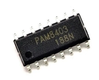
 PAM8403音频功率放大器:资料手册参数分析

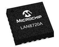
 LAN8720以太网收发器:资料手册参数分析

 SI2301 N沟道MOSFET:资料手册参数分析

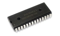
 ADC0809逐次逼近寄存器型模数转换器:资料手册参数分析
