
| 型号 | 品牌 | 获取价格 | 描述 | 数据表 |
| 4231-T110-K0F1H-15A | ETA |
获取价格 |
断路器磁性(液力延迟)15A120VAC50VDC按片DIN轨道 |

|
| 4231-T110-K0F2H-10A | ETA |
获取价格 |
断路器磁性(液力延迟)10A120VAC50VDC按片DIN轨道 |
|
| 4231-T110-K0F2H-12A | ETA |
获取价格 |
额定电流(A):12A;额定直流电压(V):50 V;额定交流电压(V):120 V;断路 |
|
| 4231-T110-K0F2H-15A | ETA |
获取价格 |
额定电流(A):15A;额定直流电压(V):50 V;额定交流电压(V):120 V;断路 |
|
| 4231-T110-K0F2H-1A | ETA |
获取价格 |
断路器磁性(液力延迟)1A120VAC50VDC按片DIN轨道 |
|
| 4231-T110-K0F2H-2A | ETA |
获取价格 |
额定电流(A):2A;额定直流电压(V):50 V;额定交流电压(V):120 V;断路器 |
|
| 4231-T110-K0F2H-3A | ETA |
获取价格 |
断路器磁性(液力延迟)3A120VAC50VDC按片DIN轨道 |
|
| 4231-T110-K0F2H-5A | ETA |
获取价格 |
断路器磁性(液力延迟)5A120VAC50VDC按片DIN轨道 |
|
| 4231-T110-K0F2H-7A | ETA |
获取价格 |
断路器磁性(液力延迟)7A120VAC50VDC按片DIN轨道 |
|
| 4231-T110-K0F2H-8A | ETA |
获取价格 |
额定电流(A):8A;额定直流电压(V):50 V;额定交流电压(V):120 V;断路器 |
|
 英伟达或将首发台积电A16工艺 芯片双雄合作再掀风云

 三星2nm芯片量产在即 半导体行业格局或将重塑
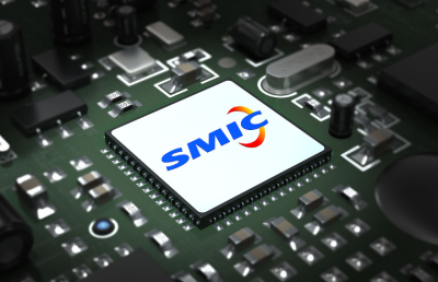
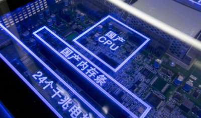 国产AI算力崛起!阿里百度用自研芯片开启AI新时代
 中国三大运营商全面布局eSIM业务 用户何时能用上?
工作时间:9:00-21:00
CEO邮箱:ceo@jiepei.com
投诉邮箱:tousu@jiepei.com


 浙公网安备 33010502006866号 浙ICP备10014259号-119
营业执照ICP证
浙公网安备 33010502006866号 浙ICP备10014259号-119
营业执照ICP证


