
 5秒后页面跳转

| 是否Rohs认证: | 符合 | 生命周期: | Obsolete |
| Reach Compliance Code: | unknown | 风险等级: | 5.84 |
| 湿度敏感等级: | 1 | Base Number Matches: | 1 |
| 型号 | 品牌 | 获取价格 | 描述 | 数据表 |
| XC66DC2930MR | TOREX |
获取价格 |
Regulator |

|
| XC66DC2931ML | TOREX |
获取价格 |
Regulator |
|
| XC66DC2932ML | TOREX |
获取价格 |
Regulator |
|
| XC66DC2932MR | TOREX |
获取价格 |
Regulator |
|
| XC66DC2933ML | TOREX |
获取价格 |
Regulator |
|
| XC66DC2936ML | TOREX |
获取价格 |
Regulator |
|
| XC66DC2937ML | TOREX |
获取价格 |
Regulator |
|
| XC66DC2937MR | TOREX |
获取价格 |
Regulator |
|
| XC66DC2938ML | TOREX |
获取价格 |
Regulator |
|
| XC66DC2938MR | TOREX |
获取价格 |
Regulator |
|
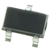 SZNUP2105LT1G电气参数、产品特性详解

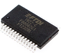 FT232RL资料解读:引脚说明、参数详情、产品特性
 RC0402FR-07100KL资料解读:电气参数、产品特性
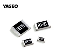 RC0603FR-070R数据手册解读:特性、应用与替换型号推荐
工作时间:9:00-21:00
CEO邮箱:ceo@jiepei.com
投诉邮箱:tousu@jiepei.com


 浙公网安备 33010502006866号 浙ICP备10014259号-119
营业执照ICP证
浙公网安备 33010502006866号 浙ICP备10014259号-119
营业执照ICP证


