
 5秒后页面跳转

| 是否无铅: | 含铅 | 是否Rohs认证: | 不符合 |
| 生命周期: | Active | 零件包装代码: | BGA |
| 包装说明: | BGA, BGA668,26X26,40 | 针数: | 668 |
| Reach Compliance Code: | not_compliant | ECCN代码: | 3A991.D |
| HTS代码: | 8542.39.00.01 | Factory Lead Time: | 12 weeks |
| 风险等级: | 5.23 | 最大时钟频率: | 1181 MHz |
| JESD-30 代码: | S-PBGA-B668 | JESD-609代码: | e0 |
| 长度: | 27 mm | 湿度敏感等级: | 4 |
| 可配置逻辑块数量: | 1368 | 输入次数: | 320 |
| 逻辑单元数量: | 12312 | 输出次数: | 320 |
| 端子数量: | 668 | 最高工作温度: | 85 °C |
| 最低工作温度: | 组织: | 1368 CLBS | |
| 封装主体材料: | PLASTIC/EPOXY | 封装代码: | BGA |
| 封装等效代码: | BGA668,26X26,40 | 封装形状: | SQUARE |
| 封装形式: | GRID ARRAY | 峰值回流温度(摄氏度): | 225 |
| 可编程逻辑类型: | FIELD PROGRAMMABLE GATE ARRAY | 认证状态: | Not Qualified |
| 座面最大高度: | 2.85 mm | 子类别: | Field Programmable Gate Arrays |
| 最大供电电压: | 1.26 V | 最小供电电压: | 1.14 V |
| 标称供电电压: | 1.2 V | 表面贴装: | YES |
| 技术: | CMOS | 温度等级: | OTHER |
| 端子面层: | Tin/Lead (Sn63Pb37) | 端子形式: | BALL |
| 端子节距: | 1 mm | 端子位置: | BOTTOM |
| 处于峰值回流温度下的最长时间: | 30 | 宽度: | 27 mm |
| Base Number Matches: | 1 |
| 型号 | 品牌 | 替代类型 | 描述 | 数据表 |
| XC4VFX12-10FF668I | XILINX |
完全替代  |
Field Programmable Gate Array, 1368 CLBs, 1028MHz, 12312-Cell, CMOS, PBGA668, FBGA-668 |

|
| XC4VFX12-11FFG668C | XILINX |
完全替代 |
Field Programmable Gate Array, 1368 CLBs, 1181MHz, 12312-Cell, CMOS, PBGA668, LEAD FREE, F |
|
| 型号 | 品牌 | 获取价格 | 描述 | 数据表 |
| XC4VFX12-11FF668I | XILINX |
获取价格 |
Field Programmable Gate Array, 1368 CLBs, 1181MHz, 12312-Cell, CMOS, PBGA668, FBGA-668 |
|
| XC4VFX12-11FF676C | XILINX |
获取价格 |
Field Programmable Gate Array, 12312-Cell, CMOS, PBGA676, |
|
| XC4VFX12-11FF676I | XILINX |
获取价格 |
Field Programmable Gate Array, 12312-Cell, CMOS, PBGA676, |
|
| XC4VFX12-11FFG668C | XILINX |
获取价格 |
Field Programmable Gate Array, 1368 CLBs, 1181MHz, 12312-Cell, CMOS, PBGA668, LEAD FREE, F |
|
| XC4VFX12-11FFG668CS1 | XILINX |
获取价格 |
Field Programmable Gate Array, 1181MHz, 12312-Cell, CMOS, PBGA668, |
|
| XC4VFX12-11FFG668I | XILINX |
获取价格 |
Field Programmable Gate Array, 1368 CLBs, 1181MHz, 12312-Cell, CMOS, PBGA668, LEAD FREE, F |
|
| XC4VFX12-11FFG676C | XILINX |
获取价格 |
Field Programmable Gate Array, 12312-Cell, CMOS, PBGA676, |
|
| XC4VFX12-11FFG676I | XILINX |
获取价格 |
Field Programmable Gate Array, 12312-Cell, CMOS, PBGA676, |
|
| XC4VFX12-11SF363C | XILINX |
获取价格 |
Field Programmable Gate Array, 1368 CLBs, 1181MHz, 12312-Cell, CMOS, PBGA363, FBGA-363 |
|
| XC4VFX12-11SF363CS1 | XILINX |
获取价格 |
Field Programmable Gate Array, 1181MHz, 12312-Cell, CMOS, PBGA363, |
|
 ULC1001数据手册解读:产品特性、替换型号推荐

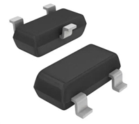 解读2N7002LT1G数据手册:特性、参数详情与引脚信息
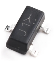 BSS138手册解读:产品特性、封装与引脚信息详解
 CSFM101数据手册:电气参数、替换型号推荐
工作时间:9:00-21:00
CEO邮箱:ceo@jiepei.com
投诉邮箱:tousu@jiepei.com


 浙公网安备 33010502006866号 浙ICP备10014259号-119
营业执照ICP证
浙公网安备 33010502006866号 浙ICP备10014259号-119
营业执照ICP证


