tance on the output line. The rising edge of an output pulse
is determined by the RC time constant of the pull-up resistor
and the stray capacitance.
causing the output pulse to last one clock period. The
minimum practical pulse width of the one-shot circuit is
approximately 100ns. Using COS to generate shorter output
pulses does not affect the output frequency or the gain
equation.
The synchronized nature of the VFC101 makes viewing its
output on an oscilloscope somewhat tricky. Since all output
pulses align with the clock, it is best to trigger and view the
clock on one of the input channels and the output can then
be viewed on another oscilloscope channel. Depending on
the VFC input voltage, the output waveform may appear as
if the oscilloscope is not properly triggered. The output
might best be visualized by imagining a constant output
frequency which is locked to a submultiple of the clock
frequency with occasional extra pulses or missing pulses to
create the necessary average frequency. It is these extra or
missing pulses that make the output waveform appear as if
the oscilloscope is not properly triggered. This behavior
amounts to a frequency or phase jitter in the output, making
frequency detection with most phase-locked loop circuitry
impractical. For the same reason, fast period measurement
(ratiometric counting) will not provide a stable reading. The
output frequency must be measured (averaged) for N counts
of fCLOCK to achieve a stable N counts of resolution.
REFERENCE VOLTAGE
Low gain drift is achieved with a precision internal 5V
reference. This reference is brought to an external pin and
can be used for a variety of purposes. It is used to offset the
noninverting comparator input in voltage-to-frequency mode
(although a precise voltage is not required for this function).
It is very useful in many other applications such as offsetting
the input to accept bipolar input signals. It can source up to
10mA and sink 100µA. Heavy loading of the reference will
change the gain of the VFC. A 10mA load interacting with
a 0.5Ω typical output impedance will change the VFC gain
equation and reference voltage by 0.1%.
LINEARITY PERFORMANCE
The linearity of the VFC100 is specified as the worst-case
deviation from a straight line defined by low scale and high
scale end point measurements. This worst-case deviation is
expressed as a percentage of the 10V full-scale input. All
units are tested.
SHORTENED OUTPUT PULSES
With pin 12 connected to +VCC, the negative output pulse
duration is equal to one period of the clock input. Shorter
output pulses may be useful in driving optical couplers or
transformers for voltage isolation or noise rejection. This
can be accomplished by connecting capacitor COS as shown
in Figure 4. Output pulses cannot be made to exceed one
clock period in duration. Thus, a COS value which would
create an output pulse which is longer than one period of the
clock will have the same effect as disabling the one-shot,
Linearity performance and gain error change with full-scale
operating frequency as shown in the typical performance
curves. Integrator voltage swing (determined by CINT) has a
minor effect on linearity. A small integrator voltage swing
typically leads to best linearity performance.
The best linearity performance at high full-scale frequencies
(above 500kHz) is obtained by using short output pulses
+VCC
1µF
2
14
fOUT
0.1µF
Output
One-Shot
0.01µF
1000pF
100pF
10pF
15
Digital
Common
tO
12
COS
11
100ns
1µs
10µs
100µs
1ms
10ms
0.1µF
Nominal Output Pulse Width, tO
+VCC
–VCC
Clock
fOUT
tO
Output Pulse Width With
Pin 12 Connected to +VCC
.
FIGURE 4. Circuit and Timing Diagram for Shortened Output Pulses.
®
VFC101
7


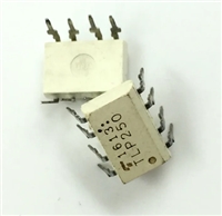
 TLP250光耦合器:资料手册参数分析

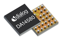
 DA14580 低功耗蓝牙系统级芯片(SoC):资料手册参数分析

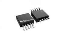
 INA226 高精度电流和功率监控器:资料手册参数分析

 SI2302 N沟道MOSFET:资料手册参数分析
