
 5秒后页面跳转

| 是否Rohs认证: | 符合 | 生命周期: | Transferred |
| 包装说明: | 13 X 15 MM, LEAD FREE, PLASTIC, BGA-165 | Reach Compliance Code: | compliant |
| 风险等级: | 5.78 | 最长访问时间: | 0.45 ns |
| JESD-30 代码: | R-PBGA-B165 | JESD-609代码: | e1 |
| 长度: | 15 mm | 内存密度: | 37748736 bit |
| 内存集成电路类型: | QDR SRAM | 内存宽度: | 9 |
| 功能数量: | 1 | 端子数量: | 165 |
| 字数: | 4194304 words | 字数代码: | 4000000 |
| 工作模式: | SYNCHRONOUS | 最高工作温度: | 70 °C |
| 最低工作温度: | 组织: | 4MX9 | |
| 封装主体材料: | PLASTIC/EPOXY | 封装代码: | LBGA |
| 封装形状: | RECTANGULAR | 封装形式: | GRID ARRAY, LOW PROFILE |
| 并行/串行: | PARALLEL | 峰值回流温度(摄氏度): | NOT SPECIFIED |
| 认证状态: | Not Qualified | 座面最大高度: | 1.51 mm |
| 最大供电电压 (Vsup): | 1.9 V | 最小供电电压 (Vsup): | 1.7 V |
| 标称供电电压 (Vsup): | 1.8 V | 表面贴装: | YES |
| 技术: | CMOS | 温度等级: | COMMERCIAL |
| 端子面层: | TIN SILVER COPPER | 端子形式: | BALL |
| 端子节距: | 1 mm | 端子位置: | BOTTOM |
| 处于峰值回流温度下的最长时间: | NOT SPECIFIED | 宽度: | 13 mm |
| Base Number Matches: | 1 |
| 型号 | 品牌 | 描述 | 获取价格 | 数据表 |
| UPD44325092F5-E40Y-EQ2 | NEC | QDR SRAM, 4MX9, 0.45ns, CMOS, PBGA165, 13 X 15 MM, PLASTIC, BGA-165 |
获取价格 |

|
| UPD44325092F5-E40Y-EQ2-A | NEC | QDR SRAM, 4MX9, 0.45ns, CMOS, PBGA165, 13 X 15 MM, LEAD FREE, PLASTIC, BGA-165 |
获取价格 |
|
| UPD44325092F5-E50-EQ2 | NEC | 36M-BIT QDRII SRAM 2-WORD BURST OPERATION |
获取价格 |
|
| UPD44325092F5-E50-EQ2-A | NEC | QDR SRAM, 4MX9, 0.45ns, CMOS, PBGA165, 13 X 15 MM, LEAD FREE, PLASTIC, BGA-165 |
获取价格 |
|
| UPD44325094BF5-E33-FQ1 | RENESAS | 4MX9 QDR SRAM, 0.45ns, PBGA165, 15 X 17 MM, PLASTIC, BGA-165 |
获取价格 |
|
| UPD44325094BF5-E33Y-FQ1 | RENESAS | 4MX9 QDR SRAM, 0.45ns, PBGA165, 15 X 17 MM, PLASTIC, BGA-165 |
获取价格 |
|
 74LS138 3-to-8线解码器/多路复用器:资料手册参数分析

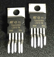 TDA2030音频功率放大器:资料手册参数分析
 74HC595移位寄存器芯片:参数深入解析与应用实践指南
 AO3401场效应管参数、引脚图、应用原理图
工作时间:9:00-21:00
CEO邮箱:ceo@jiepei.com
投诉邮箱:tousu@jiepei.com


 浙公网安备 33010502006866号 浙ICP备10014259号-119
营业执照ICP证
浙公网安备 33010502006866号 浙ICP备10014259号-119
营业执照ICP证


