NMOS linear image sensor S3902/S3903 series
Terminal
Input or output
Description
Pulses for operating the MOS shift register. The video data rate is
equal to the clock pulse frequency since the video output signal is
obtained synchronously with the rise of φ2 pulse.
Pulse for starting the MOS shift register operation. The time interval
between start pulses is equal to the signal accumulation time.
Connected to the anode of each photodiode. This should be
grounded.
Input
(CMOS logic compatible)
φ1, φ2
φst
Input
(CMOS logic compatible)
Vss
-
Vscg
Vscd
Input
Input
Used for restricting blooming. This should be grounded.
Used for restricting blooming. This should be biased at a voltage
equal to the video bias voltage.
Video output signal. Connects to photodiode cathodes when the
address is on. A positive voltage should be applied to the video
line in order to use photodiodes with a reverse voltage. When the
amplitude of φ1 and φ2 is 5 V, a video bias voltage of 2 V is
recommended.
Active video
Output
This has the same structure as the active video, but is not
connected to photodiodes, so only spike noise is output. This
should be biased at a voltage equal to the active video or left as an
open-circuit when not needed.
Dummy video
Output
-
Vsub
Connected to the silicon substrate. This should be grounded.
This should be pulled up at 5 V by using a 10 kΩ resistor. This is a
negative going pulse that appears synchronously with the φ2
timing right after the last photodiode is addressed.
Should be grounded.
Output
(CMOS logic compatible)
End of scan
NC
-
Figure 5 Spectral response (typical example)
Figure 6 Output charge vs. exposure
(Typ. Vb=2 V, V =5 V, light source: 2856 K)
(Ta=25 ˚C)
102
0.3
101
SATURATION
CHARGE
0.2
0.1
0
100
S3902 SERIES
10–1
S3903 SERIES
10–2
SATURATION EXPOSURE
10–3
10–5
10–4
10–3
10–2
10–1
100
1200
200
1000
400
800
600
EXPOSURE (lx · s)
WAVELENGTH (nm)
KMPDB0117EA
KMPDB0149EA
ꢀꢀConstruction of image sensor
Each cell consists of an active photodiode and a dummy
photodiode, which are respectively connected to the active
video line and the dummy video line via a switching transis-
tor. Each of the active photodiodes is also connected to the
saturation control drain via the saturation control transistor,
so that the photodiode blooming can be suppressed by
grounding the saturation control gate. Applying a pulse sig-
nal to the saturation control gate triggers all reset. (See “Aux-
iliary functions”.)
Figure 2 shows the schematic diagram of the photodiode
active area. This active area has a PN junction consisting of
an N-type diffusion layer formed on a P-type silicon substrate.
A signal charge generated by light input accumulates as a
capacitive charge in this PN junction. The N-type diffusion
layer provides high UV sensitivity but low dark current.
The NMOS image sensor consists of a scanning circuit made
up of MOS transistors, a photodiode array, and a switching
transistor array that addresses each photodiode, all integrated
onto a monolithic silicon chip. Figure 1 shows the circuit of a
NMOS linear image sensor.
The MOS scanning circuit operates at low power consump-
tion and generates a scanning pulse train by using a start
pulse and 2-phase clock pulses in order to turn on each ad-
dress sequentially. Each address switch is comprised of an
NMOS transistor using the photodiode as the source, the
video line as the drain and the scanning pulse input section
as the gate.
The photodiode array operates in charge integration mode
so that the output is proportional to the amount of light expo-
sure (light intensity × integration time).


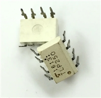
 TLP250光耦合器:资料手册参数分析

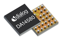
 DA14580 低功耗蓝牙系统级芯片(SoC):资料手册参数分析

 INA226 高精度电流和功率监控器:资料手册参数分析

 SI2302 N沟道MOSFET:资料手册参数分析
