
| 型号 | 品牌 | 获取价格 | 描述 | 数据表 |
| PGA281AIPW | TI |
获取价格 |
Precision, Zero-Drift, High-Voltage, Programmable Gain Instrumentation Amplifier |

|
| PGA281AIPWR | TI |
获取价格 |
Precision, Zero-Drift, High-Voltage, Programmable Gain Instrumentation Amplifier |
|
| PGA281M622C1-1921F | AMPHENOL |
获取价格 |
IC Socket, PGA281, 281 Contact(s), 2.54mm Term Pitch, 0.1inch Row Spacing, |
|
| PGA281M623C1-1921F | AMPHENOL |
获取价格 |
IC Socket, PGA281, 281 Contact(s), 2.54mm Term Pitch , 0.1inch Row Spacing |
|
| PGA289M622C1-1701F | AMPHENOL |
获取价格 |
IC Socket, PGA289, 289 Contact(s), 2.54mm Term Pitch , 0.1inch Row Spacing |
|
| PGA289M623C1-1701F | AMPHENOL |
获取价格 |
IC Socket, PGA289, 289 Contact(s), 2.54mm Term Pitch , 0.1inch Row Spacing |
|
| PGA299H003B1-2010R | AMPHENOL |
获取价格 |
IC Socket, PGA299, 299 Contact(s) |
|
| PGA299H004B1-2010R | AMPHENOL |
获取价格 |
IC Socket, PGA299, 299 Contact(s) |
|
| PGA299H008B5-2010R | AMPHENOL |
获取价格 |
IC Socket, PGA299, 299 Contact(s), |
|
| PGA299H009B5-2010R | AMPHENOL |
获取价格 |
IC Socket, PGA299, 299 Contact(s) |
|
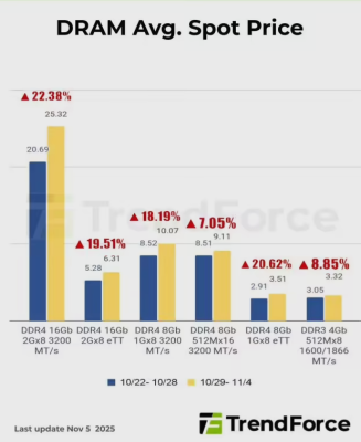 内存市场惊现抢购潮!DDR5芯片一周暴涨30%背后暗藏什么玄机?

 京东1号车震撼下线:10万内超500km续航国民车来了
 华邦电预警:内存结构性缺货将持续至2027年,AI需求引爆存储涨价潮
 英伟达联手德国电信豪掷10亿欧元 打造欧洲AI算力新标杆
工作时间:9:00-21:00
CEO邮箱:ceo@jiepei.com
投诉邮箱:tousu@jiepei.com


 浙公网安备 33010502006866号 浙ICP备10014259号-119
营业执照ICP证
浙公网安备 33010502006866号 浙ICP备10014259号-119
营业执照ICP证


