
 5秒后页面跳转

| 型号 | 品牌 | 描述 | 获取价格 | 数据表 |
| PCF8563T | NXP | Real-time clock/calendar |
获取价格 |

|
| PCF8563T/5 | NXP | Real-time clock/calendar |
获取价格 |
|
| PCF8563T/F4 | NXP | Real-time clock/calendar |
获取价格 |
|
| PCF8563T5 | NXP | Real-time clock/calendar |
获取价格 |
|
| PCF8563T-5 | NXP | Real-time clock/calendar |
获取价格 |
|
| PCF8563TD | NXP | I2C Demonstration Board 2005-1 Quick Start Guide |
获取价格 |
|
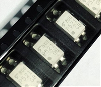 TLP521资料手册解读:参数分析、引脚说明、典型电路

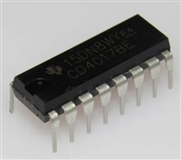 CD4017数据手册解析:参数分析、引脚说明、功能说明
 pcf8563芯片功能说明、参数分析、引脚说明
 TDA2822资料手册:引脚说明、参数分析
工作时间:9:00-21:00
CEO邮箱:ceo@jiepei.com
投诉邮箱:tousu@jiepei.com


 浙公网安备 33010502006866号 浙ICP备10014259号-119
营业执照ICP证
浙公网安备 33010502006866号 浙ICP备10014259号-119
营业执照ICP证


