
 5秒后页面跳转

| 型号 | 品牌 | 替代类型 | 描述 | 数据表 |
| NTHS5441T1G | ONSEMI |
类似代替  |
−20 V, −5.3 A, P−Channel ChipFET |

|
| 型号 | 品牌 | 获取价格 | 描述 | 数据表 |
| NTHS5441T1/D | ETC |
获取价格 |
Power MOSFET P-Channel ChipFET |
|
| NTHS5441T1G | ONSEMI |
获取价格 |
−20 V, −5.3 A, P−Channel ChipFET |
|
| NTHS5443 | ONSEMI |
获取价格 |
Power MOSFET |
|
| NTHS5443T1 | ONSEMI |
获取价格 |
Power MOSFET |
|
| NTHS5443T1 | ROCHESTER |
获取价格 |
3600mA, 20V, P-CHANNEL, Si, SMALL SIGNAL, MOSFET, CASE 1206A-03, CHIPFET-8 |
|
| NTHS5443T1/D | ETC |
获取价格 |
Power MOSFET P-Channel ChipFET? |
|
| NTHS5443T1G | ONSEMI |
获取价格 |
Power MOSFET |
|
| NTHS5443T1G | ROCHESTER |
获取价格 |
3600mA, 20V, P-CHANNEL, Si, SMALL SIGNAL, MOSFET, LEAD FREE, CASE 1206A-03, CHIPFET-8 |
|
| NTHS5445T1 | ONSEMI |
获取价格 |
Power MOSFET P−Channel ChipFET-TM |
|
| NTHS5445T1/D | ETC |
获取价格 |
Power MOSFET P-Channel ChipFET? |
|
 LTC1151C双通道±15V零漂移运算放大器全面解读

 CNX36手册解读:产品特性、应用及封装引脚详解
 PS9552资料解读:引脚信息、电气参数
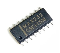 解读MAX232数据手册:全面剖析与应用推荐
工作时间:9:00-21:00
CEO邮箱:ceo@jiepei.com
投诉邮箱:tousu@jiepei.com


 浙公网安备 33010502006866号 浙ICP备10014259号-119
营业执照ICP证
浙公网安备 33010502006866号 浙ICP备10014259号-119
营业执照ICP证


