MP18831
Isolated, Dual-Input Control,
High-Side/Low-Side Half-Bridge Gate Driver
DESCRIPTION
FEATURES
The MP18831 is an isolated, half-bridge gate
driver solution with up to 4A of source and sink
peak current capability. The gate driver is
designed to drive power switching devices with
a short propagation delay and minimal pulse-
width distortion. By utilizing MPS’s proprietary
capacitive-based isolation technology, the
driver can provide up to 5kVRMS withstand
voltage (per UL 1577) (SOIC wide-body
package option). It can also provide a common-
mode transient immunity (CMTI) rating above
100kV/µs between the input side and output
driver. These advanced features enable high
efficiency, high power density, and robustness
in a wide variety of power applications.
• Up to 5kVRMS Input to Output Isolation
(SOIC-16 WB Package)
• 1500VDC Functional Isolation between Two
Secondary-Side Drivers (SOIC-16 NB and
SOIC-16 WB Packages)
• 700VDC Functional Isolation between Two
Secondary-Side Drivers (LGA-13 Package)
• Common-Mode Transient Immunity (CMTI)
>100kV/µs
• 2.8V to 5.5V Input VDDI Voltage (VDDI
)
Range to Interface with TTL and CMOS-
Compatible Inputs
• Up to 30V Output Drive Supply with Several
Under-Voltage Lockout (UVLO) Options
• 4A Source, 4A Sink Peak Current Output
• 50ns Typical Propagation Delay
• Overlap Protection and Configurable Dead
Time (DT) Control
• -40°C to +125°C Operating Temperature
Range
• UL 1577 Certified:
• SOIC-16 NB: 3kVRMS Isolation for 60s
• SOIC-16 WB: 5kVRMS Isolation for 60s
• LGA-13: 2.5kVRMS Isolation for 60s
• DIN EN IEC 60747-17 (VDE 0884-17): 2021-
10 Certified
The MP18831 integrates dual-channel gate
drivers in one package. Each output can be
grounded to the separated grounds, or
connected to a positive or negative voltage
reference. The secondary topology can be
configured as a half-bridge high-side (HS) and
low-side (LS) driver, which are each controlled
by two independent input signals. To prevent
shoot-through in the half-bridge driver, the
MP18831 provides a configurable dead time
(DT) set via an external resistor.
A wide primary-side VDDI supply voltage (VDDI
)
• SOIC-16 NB: 4242VPK Isolation
• SOIC-16 WB: 6000VPK Isolation
• LGA-13: 3535VPK Isolation
range makes the driver suitable to be interfaced
with 3.3V and 5V digital controllers. The
secondary-side driver can accept up to a 30V
supply. All of the supply voltage pins feature
• CQC Certification per GB 4943.1-2011
• Available in SOIC-16 NB, SOIC-16 WB, and
LGA-13 (5mmx5mm) Packages
multiple
under-voltage
lockout
(UVLO)
protection options.
APPLICATIONS
The MP18831 is available in SOIC-16 NB
(narrow body), SOIC-16 WB (wide body), and
LGA-13 (5mmx5mm) packages.
• Half/Full-Bridge Converters
• Isolated DC/DC Converters
• Offline Isolated AC/DC Converters
• DC/AC Inverters
All MPS parts are lead-free, halogen-free, and adhere to the RoHS directive.
For MPS green status, please visit the MPS website under Quality
Assurance. “MPS”, the MPS logo, and “Simple, Easy Solutions” are
trademarks of Monolithic Power Systems, Inc. or its subsidiaries.
MP18831 Rev. 1.0
7/26/2022
MonolithicPower.com
MPS Proprietary Information. Patent Protected. Unauthorized Photocopy and Duplication Prohibited.
© 2022 MPS. All Rights Reserved.
1

 5秒后页面跳转


 NE5532双低噪声运算放大器:资料手册参数分析

 74LS138 3-to-8线解码器/多路复用器:资料手册参数分析
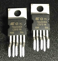 TDA2030音频功率放大器:资料手册参数分析
 74HC595移位寄存器芯片:参数深入解析与应用实践指南


 浙公网安备 33010502006866号 浙ICP备10014259号-119
营业执照ICP证
浙公网安备 33010502006866号 浙ICP备10014259号-119
营业执照ICP证


