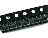
ML145554, ML145557, ML145564, ML145567
LANSDALE Semiconductor, Inc.
serial PCM word, clocked by BCLK , out of D . If the FS
X
amplifier pair can drive 300 Ω to 3.3 V peak.
X
X
pulse is high for more than eight BCLK periods, the D and
X
X
TS outputs will remain in a low–impedance state until FS is POWER SUPPLY
X
X
brought low. The length of the FS pulse is used to determine
X
whether the transmit and receive digital I/O conforms to the
Short Frame Sync or to the Long Frame Sync convention.
GNDA
Analog Ground
This terminal is the reference level for all signals, both ana-
log and digital. It is 0 V.
TSX
Transmit Time Slot Indicator
This is an open–drain output that goes low whenever the D
output is in a low–impedance state (i.e., during the transmit
time slot when the PCM word is being output) for enabling a
PCM bus driver.
V
X
CC
Positive Power Supply
V
CC
is typically 5 V.
V
BB
Negative Power Supply
ANLB
Analog Loopback Control Input (ML145564/67 Only)
V
BB
is typically – 5 V.
When held high, this pin causes the input of the transmit RC
active filter to be disconnected from GS and connected to
X
FUNCTIONAL DESCRIPTION
VPO+ for analog loopback testing. This pin is held low in
normal operation.
ANALOG INTERFACE AND SIGNAL PATH
ANALOG
The transmit portion of these codec–filters includes a
low–noise gain setting amplifier capable of driving a 600 Ω
load. Its output is fed to a three–pole anti–aliasing pre–filter.
This pre–filter incorporates a two–pole Butterworth active
low–pass filter, and a single passive pole. This pre–filter is
followed by a single ended–to–differential converter that is
clocked at 256 kHz. All subsequent analog processing uti-
lizes fully differential circuitry. The next section is a
fully–differential, five–pole switched capacitor low–pass fil-
ter with a 3.4 kHz passband. After this filter is a 3–pole
switched–capacitor high–pass filter having a cutoff frequen-
cy of about 200 Hz. This high–pass stage has a transmission
zero at DC that eliminates any DC coming from the analog
input or from accumulated operational amplifier offsets in
the preceding filter stages. The last stage of the high–pass
filter is an autozeroed sample and hold amplifier.
GS
X
Gain–Setting Transmit
This output of the transmit gain–adjust operational amplifi-
er is internally connected to the encoder section of the device.
It must be used in conjunction with VFXI– and VFXI+ to set
the transmit gain for a maximum signal amplitude of 2.5 V
peak. This output can drive a 600 Ω load to 2.5 V peak.
VF I–
X
Voice–Frequency Transmit Input (Inverting)
This is the inverting input of the transmit gain–adjust
operational amplifier.
VF I+
X
One bandgap voltage reference generator and
Voice–Frequency Transmit Input (Non–Inverting)
digital–to–analog converter (DAC) are shared by the transmit
and receive sections. The autozeroed, switched–capacitor
bandgap reference generates precise positive and negative
reference voltages that are independent of temperature and
power supply voltage. A binary–weighted capacitor array
(CDAC) forms the chords of the companding structure,
while a resistor string (RDAC) implements the linear steps
within each chord. The encode process uses the DAC, the
voltage reference, and a frame–by–frame autozeroed com-
parator to implement a successive–approximation conversion
algorithm. All of the analog circuitry involved in the data
conversion the voltage reference, RDAC, CDAC, and com-
parator are implemented with a differential architecture.
The receive section includes the DAC described above,
asample and hold amplifier, a five–pole 3400 Hz switched-
capacitor low–pass filter with sinX/X correction, and a
two–pole active smoothing filter to reduce the spectral com-
ponents of the switched capacitor filter. The output of the
smoothing filter is a power amplifier that is capable of driv-
ing a 600 Ω load. The ML145564 and ML145567 add a pair
of power amplifiers that are connected in a push–pull con-
figuration; two external resistors set the gain of both of the
This is the non–inverting input of the transmit gain–adjust
operational amplifier.
VF O
R
Voice–Frequency Receive Output
This receive analog output is capable of driving a 600 Ω load
to 2.5 V peak.
VPI
Voltage Power Input (ML145564/67 Only)
This is the inverting input to the first receive power ampli-
fier. Both of the receive power amplifiers can be powered
down by connecting this input to V
.
BB
VPO–
Voltage Power Output (Inverted) (ML145564/67 Only)
This inverted output of the receive push–pull power ampli-
fiers can drive 300 Ω to 3.3 V peak.
VPO+
Voltage Power Output (Non–Inverted) (ML145554/67 Only)
This non–inverted output of the receive push–pull power
Page 4 of 18
www.lansdale.com
Issue A


 一文带你解读74HC244资料手册:特性、应用场景、封装方式、引脚配置说明、电气参数、推荐替代型号

 AD623资料手册解读:特性、应用、封装、引脚功能及电气参数

 RT9193资料手册解读:RT9193引脚功能、电气参数、替换型号推荐

 VIPER22A的资料手册解读、引脚参数说明、代换型号推荐
