Freescale Semiconductor, Inc.
Table A–5 DC Characteristics (Continued)
(V and V
= 5.0 Vdc ± 5%, V = 0 Vdc, T = T to T
)
H
DD
DDSYN
SS
A
L
Num
Characteristic
Symbol
Min
Max
Unit
3,16
Input Capacitance
All input-only pins except ADC pins
All input/output pins
C
in
18
—
—
10
20
pF
16
Load Capacitance
—
—
—
—
90
Group 1 I/O Pins, CLKOUT, FREEZE/QUOT, IPIPE0
Group 2 I/O Pins and CSBOOT, BG/CS
Group 3 I/O Pins
C
L
19
100
130
200
pF
Group 4 I/O Pins
NOTES:
1. Applies to:
Port ADA[7:0] — AN[7:0]
Port E[7:4] — SIZ[1:0], AS, DS
Port F[7:0] — IRQ[7:1], MODCLK
Port GP[7:0] — IC4/OC5/OC1, IC[3:1], OC[4:1]/OC1
Port QS[7:0] — TXD, PCS[3:1], PCS0/SS, SCK, MOSI, MISO
BKPT/DSCLK, DSI/IPIPE1, PAI, PCLK, RESET, RXD, TSC
EXTAL (when PLL enabled)
2. This parameter is periodically sampled rather than 100% tested.
3. Applies to all input-only pins except ADC pins.
4. Applies to all input/output and output pins
5. Does not apply to HALT and RESET because they are open drain pins. Does not apply to Port QS[7:0] (TXD,
PCS[3:1], PCS0/SS, SCK, MOSI, MISO) in wired-OR mode.
6. Applies to Group 1, 2, 4 input/output and all output pins
7. Applies to Group 1, 2, 3, 4 input/output pins, BG/CS, CLKOUT, CSBOOT, FREEZE/QUOT, and IPIPE0
8. Applies to DATA[15:0]
9. Use of an active pulldown device is recommended.
10. Total operating current is the sum of the appropriate I , I
, and I
SB
values, plus I values in-
. I
DD DDSYN
DDA DD
clude supply currents for device modules powered by V
and V
pins.
DDE DDI
11. Current measured at maximum system clock frequency, all modules active.
12. The base configuration of the MC68HC16Z1 requires a 32.768 kHz crystal reference, and the base configu-
ration of the M68HC16Z2 requires a 4.194 MHz crystal reference. Both devices can be ordered with either
crystal reference as a mask option.
13. The SRAM module will not switch into standby mode as long as V
0.5 volts. The SRAM array cannot be accessed while the module is in standby mode.
does not exceed V
by more than
SB
DD
14. When V is more than 0.3 V greater than V , current flows between the V
and V
pins, which
DD
SB DD STBY
causes standby current to increase toward the maximum transient condition specification. System noise on
the V and V pin can contribute to this condition.
DD STBY
15. Power dissipation measured at specified system clock frequency, all modules active. Power dissipation can
be calculated using the expression:
P
= Maximum V
(I
+ I
+ I ) + Maximum V
(I
pins.
)
D
DD DD
DDSYN
SB DDA DDA
I
includes supply currents for all device modules powered by V
and V
DDI
DD
16. Input-Only Pins: EXTAL, TSC, BKPT/DSCLK, PAI, PCLK, RXD
DDE
Output-Only Pins: CSBOOT, BG/CS1, CLKOUT, FREEZE/QUOT, DS0/IPIPE0, PWMA, PWMB
Input/Output Pins:
Group 1: Port GP[7:0] — IC4/OC5/OC1, IC[3:1], OC[4:1]/OC1
DATA[15:0], DSI/IPIPE1
Group 2: Port C[6:0] — ADDR[22:19]/CS[9:6], FC[2:0]/CS[5:3]
Port E[7:0] — SIZ[1:0], AS, DS, AVEC, DSACK[1:0]
Port F[7:0] — IRQ[7:1], MODCLK
Port QS[7:3] — TXD, PCS[3:1], PCS0/SS, ADDR23/CS10/ECLK
ADDR[18:0], R/W, BERR, BR/CS0, BGACK/CS2
Group 3: HALT, RESET
Group 4: MISO, MOSI, SCK
M68HC16ZEC20/D
7
For More Information On This Product,
Go to: www.freescale.com


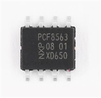
 pcf8563芯片功能说明、参数分析、引脚说明

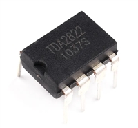
 TDA2822资料手册:引脚说明、参数分析

 TJA1050资料数据分析、引脚说明、应用示例介绍

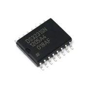
 DS3231时钟芯片:参数分析、引脚说明、应用示例介绍
