M2060/61/62, M2065/66/67
Integrated
Circuit
Systems, Inc.
VCSO FEC PLL FOR SONET/OTN
P r e l i m i n a r y I n f o r m a t i o n
M2062/67: FEC De-map LUT, Both OTU1 and OTU2
Use this option for both OTU1 or OTU2 de-mapping
applications. The Mfec divider value is kept nearly
constant to maintain similar loop bandwidth using one
set of external filter component values.
FUNCTIONAL DESCRIPTION
The M206x Series is a PLL (Phase Locked Loop) based
clock generator that generates output clocks synchro-
nized to one of two selectable input reference clocks.
An internal high "Q" SAW delay line provides low jitter
signal performance and establishes the output
frequency of the VCSO (Voltage Controlled SAW
Oscillator). In a given M206x Series device, the VCSO
center frequency is fixed. A common center frequency
is 622.08MHz, for SONET or SDH optical network
applications. The VCSO center frequency is specified at
time of order (see “Ordering Information” on pg. 12).
The VCSO has a guaranteed tuning range of ±120 ppm
(commercial temperature grade).
Fvcso =
FEC_SEL1:0
0
Base Input
Mfec Rfec
Base Output
Rate (MHz)
Description
Rate (MHz)
1
For M2062 or M2067 with Fvcso = 622.08 (OTU1 or OTU2 FEC rate):
237/255 OTU2 to OC-192 decode
0
0
1
1
0
1
0
1
79 85
79 79
84 90
84 84
669.3266 622.08
OC-192 repeater or jitter attenuator
238/255 OTU1 to OC-48 decode
OC-48 repeater or jitter attenuator
622.08
666.5143 622.08
622.08 622.08
622.08
Table 7: M2062/67: FEC De-map LUT, Both OTU1 and OTU2
P Divider Look-Up Table (LUT)
Pin selectable dividers are used within the PLL and
for the output clock. This enables tailoring of device
functionality and performance. The FEC feedback and
reference dividers (the “Mfec Divider” and “Rfec
Divider”) provide the multiplication ratios necessary to
accomodate clock translation for both forward and
inverse Forward Error Correction. The Mfec and Rfec
dividers also control the phase detector frequency. The
feedback divider (labeled “Mfin Divider”) provides the
broader division options needed to accomodate various
reference clock frequencies.
The P_SEL2:0 pins select the P divider values, which set
the output clock frequencies. P divider values of 1, 4, 8,
or 32 are available, plus a TriState mode. A P divider of
value of 1 will provide a 669.3266MHz output when using
a 669.3266MHz VCSO, for example. The outputs can be
placed into the valid state combinations as listed in
Table 8. (They cannot be set independently to any of the
available output frequencies.)
M2060-622.0800 or M2065-622.0800
P Value
forFOUT0 forFOUT1
Output Frequency (MHz)
P_SEL2:0
FOUT0
FOUT1
For example, the M2062-11-622.0800 (see “Ordering
Information” on pg. 12) has a 622.08MHz VCSO
frequency:
0
0
0
0
1
1
1
1
0
0
1
1
0
0
1
1
0
1
0
1
0
1
0
1
32
32
1
4
8
1
4
1
1
8
4
4
19.44 622.08
19.44 155.52
622.08 622.08
155.52 622.08
77.76 77.76
155.52 155.52
77.76 155.52
N/A
• The FEC de-mapper PLL ratios (in Tables 6 and 7)
enable the M2062-11-622.0800 to accept “base” input
reference frequencies of: 666.5143 (OTU1), 669.3266
(OTU2), and 622.08MHz (OC-192).
4
8
• The Mfin feedback divider enables the actual input
reference clock to be the base input frequency
divided by 1, 4, 8, or 32 (or 16). Therefore, for the base
input frequency of 622.08MHz, the actual input
reference clock frequencies can be: 622.08, 155.52,
77.76, and 19.44 or 38.88MHz. (See Tables 3 and 4 on
pg. 3.)
TriState TriState
N/A
Table 8: P Divider Look-Up Table (LUT)
General Guidelines for Phase Detector Frequency
The phase detector frequency (Fpd) is equal to the
input reference frequency (Fref) divided by the Rfec
divider value, or:
Fpd = Fref / Rfec
Key to Device Variants and Look-up Table Options
Device
General guidelines:
Look-up Table Option
Variant
Mfin Lookup Table is:
Mfec Look-up Table is:
• A lower phase detector frequency should be used for
loop timing applications to assure PLL tracking,
especially during GR-253 jitter tolerance testing. The
recommended maximum phase detector frequency
for loop timing mode is 19.44MHz.
M2060
M2061
M2062
M2065
M2066
M2067
Table 5 (FEC mapper LUT)
Table 6 (FEC de-mapper LUT)
Table 7 (FEC de-mapper LUT)
Table 5 (FEC mapper LUT)
Table 6 (FEC de-mapper LUT)
Table 7 (FEC de-mapper LUT)
Table 3
(includes divider value 32)
Table 4
(includes divider value 16)
• When LOL is to be used for system health monitoring,
the phase detector frequency should be 5MHz or
greater. Low phase detector frequencies make LOL
overly sensitive, and higher phase detector
frequencies make LOL less sensitive. The LOL pin
should not be used during loop timing mode.
Table 9: Key to Device Variants and Look-up Table Options
The P divider scales the VCSO output enabling lower
output frequency selections (Table 8).
M2060/61/62 M2065/66/67 Datasheet Rev 0.4
4 of 12
Revised 30Jul2004
Integrated Circuit Systems, Inc. ● Networking & Communications ● www.icst.com ● tel (508) 852-5400


 SI2301 N沟道MOSFET:资料手册参数分析

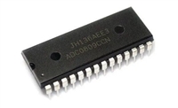
 ADC0809逐次逼近寄存器型模数转换器:资料手册参数分析

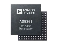
 AD9361捷变收发器:全面参数解析与关键特性概览

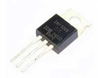
 IRF3205功率MOSFET:资料手册参数分析
