LNK500
However, in laboratory bench tests, it is often more convenient
totestthepowersupplyoutputcharacteristicstartingfromalow
output current and gradually increasing the load. In this case,
the optocoupler feedback regulates the output voltage until the
peakoutputpowercurveisreachedasshowninFigure8. Under
these conditions, the output current will continue to rise until
the peak power point is reached and the optocoupler turns off.
Once the optocoupler is off, the CONTROL pin feedback
current is determined only by R1 and R3 and the output current
therefore folds back to the inherent CC characteristic as shown.
Since this type of load transition does not normally occur in a
batterycharger,theoutputcurrentneverovershootstheinherent
constant current value in the actual application.
The secondary of the transformer is rectified and filtered by D6
and C5 to provide the DC output to the load.
LinkSwitch dramatically simplifies the secondary side by
controlling both the constant voltage and constant current
regions entirely from the primary side. This is achieved by
monitoring the primary-side VOR (voltage output reflected).
Diode D5 and capacitor C4 form the primary clamp network.
Thisbothlimitsthepeakdrainvoltageduetoleakageinductance
and provides a voltage across C4, which is equal to the VOR plus
an error due to the parasitic leakage inductance. Resistor R2
filters the leakage inductance spike and reduces the error in the
valueoftheVOR. ResistorR1convertsthisvoltageintoacurrent
that is fed into the CONTROL pin to regulate the output.
In some applications it may be necessary to avoid any output
currentovershoot,independentofthedirectionof loadvariation.
To achieve this goal, the minimum voltage feedback threshold
should be set at VO(MAX). This will ensure that the voltage at the
CC to CV transition point of the inherent characteristic will
always occur below the voltage feedback threshold. However,
theoutputvoltagetoleranceisthenincreased, sincetheinherent
CV characteristic tolerance below VO(MAX) is added to the
tolerance of the optocoupler feedback circuit.
During CV operation the output is regulated through control of
the duty cycle. As the current into the CONTROL pin exceeds
approximately 2 mA, the duty cycle begins to reduce, reaching
30% at a CONTROL pin current of 2.3 mA.
Under light or no-load conditions, when the duty cycle reaches
approximately 4%, the switching frequency is reduced to lower
energy consumption.
Applications Example
If the output load is increased beyond the peak power point
(defined by 0.5·L·I2·f), the output voltage and VOR falls. The
reduced CONTROL pin current will lower the internal
LinkSwitch current limit (current limit control) providing an
approximatelyconstantcurrentoutputcharacteristic.Iftheload
is increased and the CONTROL pin current falls below
approximately 1 mA, the CONTROL pin capacitor C3 will
discharge and the supply enters auto-restart.
The circuit shown in Figure 9 shows a typical implementation
of an approximate constant voltage / constant current (CV/CC)
charger using LinkSwitch. This design delivers 2.75 W with a
nominal peak power point voltage of 5.5 V and a current of
500 mA. Efficiency is greater than 70% over an input range of
85 VAC to 265 VAC.
The bridge rectifier, BR1, rectifies the AC input. Resistor, RF1
is a fusible type providing protection from primary side short
circuits. The rectified AC is smoothed by C1 and C2 with
inductor L1 forming a pi-filter in conjunction with C1 and C2
to filter conducted EMI. The switching frequency of 42 kHz
allows such a simple EMI filter to be used without the need for
a Y capacitor while still meeting international EMI standards.
Current limit control removes the need for any secondary side
current sensing components (sense resistor, transistor, opto
coupler and associated components). Removing the secondary
sense circuit dramatically improves efficiency, giving the
associated benefit of reduced enclosure size.
Key Application Considerations
Design Output Power
When power is applied, high voltage DC appears at the DRAIN
pin of LinkSwitch (U1). The CONTROL pin capacitor C3 is then
chargedthroughaswitchedhighvoltagecurrentsourceconnected
internally between the DRAIN and CONTROL pins. When the
CONTROL pin reaches approximately 5.6 V relative to the
SOURCE pin, the internal current source is turned off. The
internalcontrolcircuitryisactivatedandthehighvoltageMOSFET
starts to switch, using the energy in C3 to power the IC.
Table 1 (front page) provides guidance for the maximum
continuous output power from a given device under the
conditions specified.
The output of chargers (CV/CC) are normally specified at the
typical output peak power point. Conversely, non-charger
applications (CV only, which applies to many converters such
as adapters, standby/auxiliary supplies and other embedded
AC-DC converters) where CC operation is not required, are
normally specified at the minimum output power they will
supply under worst case conditions.
When the MOSFET is on, the high voltage DC bus is connected
to one end of the transformer primary, the other end being
connected to primary return. As the current ramps in the
primary of flyback transformer T1, energy is stored. This
energy is delivered to the output when the MOSFET turns off
each switching cycle.
B
3/03
6


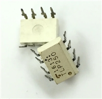
 TLP250光耦合器:资料手册参数分析

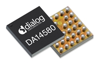
 DA14580 低功耗蓝牙系统级芯片(SoC):资料手册参数分析

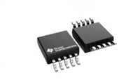
 INA226 高精度电流和功率监控器:资料手册参数分析

 SI2302 N沟道MOSFET:资料手册参数分析
