LNK500
instead placed on the cathode side of D1, it would become a
switching node, generating additional common mode EMI
currents through its internal parasitic capacitance.
transistor voltage and dissipation ratings and should be fully
tested before finalizing a design. The values of C2 and C3 are
less important other than to make sure they are large enough to
have very little influence on the impedance of the voltage
division circuit set up by R1, R3 and U1 at the switching
frequency. Normally, the values of C2 and C3 in Figure 6 are
chosen equal to the value of C2 in Figure 5, though the voltage
rating may be reduced depending on the relative values of R1
and R2 discussed above. See Applications section for typical
values of components.
The feedback configuration in Figure 6 is simply a resistive
divider made up of R1 and R3 with D1, R2, C1 and C2 rectifying,
filtering and smoothing the primary winding voltage signal. The
optocoupler therefore effectively adjusts the resistor divider ratio
to control the DC voltage across R1 and therefore, the feedback
current received by the LinkSwitch CONTROL pin.
When the power supply operates in the constant current (CC)
region, for example when charging a battery, the output voltage
isbelowthevoltagefeedbackthresholddefinedbyU1andVR1
and the optocoupler is fully off. In this region, the circuit
behaves exactly as previously described with reference to
Figure 5 where the reflected voltage increases with increasing
output voltage and the LinkSwitch internal current limit is
adjusted to provide an approximate CC output characteristic.
Note that for similar output characteristics in the CC region, the
value of R1 in Figure 5 will be equal to the value of R1+R3 in
Figure 6.
Figure 7 shows the influence of optocoupler feedback on the
output characteristic. The envelope defined by the dashed lines
represent the worst case power supply DC output voltage and
current tolerances (unit-to-unit and over the input voltage
range) if an optocoupler is not used. A typical example of an
inherent (without optocoupler) output characteristic is shown
dotted. This is the characteristic that would result if U1, R4 and
VR1 were removed. The optocoupler feedback results in the
characteristic shown by the solid line. The load variation arrow
in Figure 7 represents the locus of the output characteristic
normally seen during a battery charging cycle. The two
characteristics are identical as the output voltage rises but then
separate as shown when the voltage feedback threshold is
reached. This is the characteristic seen if the voltage feedback
threshold is above the output voltage at the inherent CC to CV
transition point also indicated in Figure 7.
When the output reaches the voltage feedback threshold set by
U1 and VR1, the optocoupler turns on. Any further increase in
the power supply output voltage results in the U1 transistor
currentincreasing,whichincreasesthepercentageofthereflected
voltage appearing across R1. The resulting increase in the
LinkSwitchCONTROLcurrentreducesthedutycycleaccording
toFigure4andtherefore,maintainstheoutputvoltageregulation.
Figure 8 shows a case where the voltage feedback threshold is
set below the voltage at the inherent CC to CV transition point.
In this case, as the output voltage rises, the secondary feedback
circuit takes control before the inherent CC to CV transition
occurs. In an actual battery charging application, this simply
limits the output voltage to a lower value.
Normally, R1 and R3 are chosen to be equal in value. However,
increasing R3 (while reducing R1 to keep R1 + R3 constant)
increasesloopgainintheCVregion,improvingloadregulation.
The extent to which R3 can be increased is limited by opto
Output Voltage
Tolerance envelope
without optocoupler
Inherent
CC to CV
transition
point
Typical inherent
characteristic without
optocoupler
Voltage
feedback
threshold
VO(MAX)
Characteristic with
optocoupler
Power supply peak
output power curve
Load variation
during battery
charging
Characteristic observed with
load variation often applied during
laboratory bench testing
Output Current
PI-2790-112102
Figure 8. Output Characteristic with Optocoupler Regulation (Reduced Voltage Feedback Threshold).
B
3/03
5


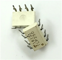
 TLP250光耦合器:资料手册参数分析

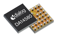
 DA14580 低功耗蓝牙系统级芯片(SoC):资料手册参数分析

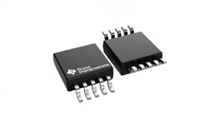
 INA226 高精度电流和功率监控器:资料手册参数分析

 SI2302 N沟道MOSFET:资料手册参数分析
