LNK454/456-458/460
IC Supply and BYPASS Pin
properly designed supply will not operate in this mode under
normal load conditions. A power supply designed correctly will
operate within the switching frequency range [fMIN … fMAX], with
an on-time falling between tON(MIN) and tON(MAX) when connected
to a normal load.
The internal 5.85 V regulator charges the bypass capacitor
connected to the BYPASS pin to 5.85 V by drawing current
from the voltage on the DRAIN pin whenever the power MOSFET
is off. The BYPASS pin is the internal supply voltage node.
When the power MOSFET is on, the device operates from the
energy stored in the bypass capacitor. Extremely low power
consumption of the internal circuitry allows LinkSwitch-PL to
operate continuously from current it takes from the DRAIN pin. A
bypass capacitor value of 1 µF is sufficient for both high
frequency decoupling and energy storage.
Overload Protection
In case of overload, the system will increase the operating
frequency and on-time each AC half-cycle until the maximum
frequency and maximum on-time are reached. When this state
is reached, by the next half-cycle, the controller will enter
auto-restart protection, thus inhibiting the gate of the power
MOSFET for approximately 1.28 s if the main line frequency is
50 Hz, 1.02 s if it is 60 Hz. After this auto-restart off-time
expires, the circuit will start again, exactly as at start-up, i.e. at
fMIN and tON(MIN), stepping up until regulation is achieved again.
In case of a persistent overload condition, the auto-restart duty
cycle DCAR will typically be as low as 33%.
During phase angle dimming when the conduction angle is
small the AC input voltage is present for only short periods of
time. In that case the IC should not rely on the integrated high
voltage current source, but instead external bias circuitry should
be used to supply the IC from the output (DES and RES in Figure
4). If the output voltage is less than 7 V, external bias circuitry
should be implemented, by using a bias winding on the primary
of the transformer with a small signal rectifier and an electrolytic
capacitor with a value based on maximum IC consumption and
maximum phase dimming conduction angles.
Auto-restart is inhibited during phase dimming when the TRIAC
conduction duty cycle is less than 60%.
Output Overvoltage Protection
If a no-load condition is present on the output of the supply, the
output overvoltage Zener (DZOV in Figure 4) will conduct once its
threshold is reached. A voltage VOV in excess of VFB(LO) = 2 V will
appear across the FEEDBACK pin and the IC will latch off. Normal
operation will be restored once the BYPASS pin voltage drops
below 4.9 V and the IC goes through a new start-up phase.
Start-up, Switching Frequency, On-time Range
At start-up the controller uses an initial switching frequency fMIN
and minimum on-time tON(MIN). The charging of the output
capacitor together with the energy delivery to the output LEDs
as soon as their anode-cathode threshold is reached
determines a step-by-step increase of the operating power
MOSFET switching frequency and on-time every half-cycle of
the main input voltage.
Output Short-Circuit
If the output of the supply (i.e. the LED load) is short-circuited,
then a large amount of energy will be delivered to the sense
resistor, generating a high voltage at the FEEDBACK pin. If this
condition develops more than 2 V on the FEEDBACK pin, then
the IC will interpret this event as an output short-circuit and will
trigger latching shutdown. Normal operation will resume after
cycling the AC input such that the BYPASS pin voltage drops
below 4.9 V and the IC goes through a new start-up phase.
When the operating conditions (start-up or large transients)
allow for only low energy processing (low frequency and on-time),
the voltage across the input bulk capacitance will not reach zero
even if the main voltage crosses zero. During these conditions the
IC sets the reference voltage on the FEEDBACK pin to one half
of its preset level (145 mV), to avoid overshoot of the output LED
current. Once the FEEDBACK pin voltage exceeds this reduced
threshold (with the zero crossing on the bulk capacitor being
achieved), then the FEEDBACK pin voltage is restored to the
normal 290 mV level.
Safe Operating Area (SOA) Protection
If 3 consecutive cycles of the power MOSFET are prematurely
terminated due to the power MOSFET current exceeding the
current limit after the leading edge blanking time, SOA protection
mode is triggered and the IC will trigger latching shutdown.
Normal operation will resume after cycling the AC input such that
the BYPASS pin voltage drops below 4.9 V and the IC goes
through a new start-up phase.
The steady state switching frequency and on-time is determined
by the line voltage, voltage drop across the LEDs and system
overall power transfer efficiency.
At light load when the device reaches the minimum frequency
fMIN and on-time tON(MIN), the controller regulates by skipping
cycles. In this mode of operation the input current is not power
factor corrected and the average output current is not
guaranteed to fall within the normal range. The FEEDBACK pin
cycle skipping threshold is reduced from approximately twice
the normal regulation level down to just above the level required
to limit output power delivery under these conditions. A
Hysteretic Thermal Shutdown
The thermal shutdown circuitry senses the die junction
temperature. The thermal shutdown threshold is set to 142 °C
typical with a 75 °C hysteresis. When the die temperature rises
above this threshold (142 °C) the power MOSFET is disabled
and remains disabled until the die temperature falls by 75 °C, at
which point the power MOSFET is re-enabled.
5
PRELIMINARY
This document contains information on a new product. Specifications and information herein
are subject to change without notice.
www.powerint.com
Rev. A 06/10


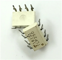
 TLP250光耦合器:资料手册参数分析

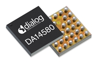
 DA14580 低功耗蓝牙系统级芯片(SoC):资料手册参数分析

 INA226 高精度电流和功率监控器:资料手册参数分析

 SI2302 N沟道MOSFET:资料手册参数分析
