LCS700-708
pulse width requirement for detection of both voltage thresholds
is nominally 30 ns. i.e. the thresholds have to be exceeded for
>30 ns for proper detection.
entering the two most sensitive pins on the list, namely the
FEEDBACK and DT/BF pins, will cause duty cycle, and dead-
time imbalance, respectively.
Over-Temperature Shutdown
Figure 5 and Figure 6 show two alternate schemes for routing
ground traces for optimum performance. Figure 5 shows a
layout footprint for the LCS with oval pads. These allow a trace
to be passed between pins 3 and 5, directly connecting the
ground systems for the bypass capacitors located on each side
of the IC.
The HiperLCS has latching OTP. VCCH must be cycled to
resume operation once the unit drops down below the OTP
threshold.
Basic Layout Guidelines
The HiperLCS is a high-frequency power device and requires
careful attention to circuit board layout in order to achieve
maximum performance.
Figure 6 shows an LCS layout footprint with round pads that do
not allow traces to be routed between them due to insufficient
space. In this case, a jumper (JP1, a 1206 size 0 W resistor) is
used to connect the ground systems together and allow a
connection for pin 3 to be routed under JP1 to the optocoupler.
The bypass capacitors need to be positioned and laid out
carefully to minimize trace lengths to the pins they serve. SMD
components are recommended for minimum component and
trace stray inductance.
Transformer T1 is a source of both high di/dt signals and dv/dt
noise. The first can couple magnetically to sensitive circuitry,
while the second can inject noise via electrostatic coupling.
Electrostatic noise coupling can be reduced by grounding the
transformer core, but it is not economically feasible to reduce
the stray magnetic field around the transformer without drastically
reducing its efficiency. Sensitive traces and components (such
as the optocoupler) should be located away from the transformer
to avoid noise pickup.
Table 2 describes the recommended bypass capacitor values
for pins that require filtering/bypassing. The table lists the pins
in the order of most to least sensitive. The bypass capacitor of
the pin at the top of the list being the most sensitive, receives
higher priority in bypass capacitor positioning to minimize trace
lengths, than the bypass capacitor of the pin below it. Noise
Pin
Returned to Pin
Recommended Value
Notes
FEEDBACK (FB)
GROUND
4.7 nF (at 250 kHz)
Increase value proportionally for lower nominal frequency (e.g. 10
nF at 100 kHz). Forms a pole with FEEDBACK pin input
impedance which is part of feedback loop characteristic. Must
not introduce excessive phase shift at expected gain
crossover frequency. Noise entering FEEDBACK pin will cause
duty cycle imbalance.
DEAD-TIME/BURST
FREQUENCY (DT/BF)
GROUND
4.7 nF
Time constant of this capacitor and the source
impedance of the resistors connected to DT/BF pin
must be <100 ms. Noise entering DT/BF pin will cause
dead time imbalance.
CURRENT SENSE (IS) GROUND
1 nF (at 250 kHz)
Value changes proportionally with nominal LLC stage
operating frequency. Forms an RC low pass filter with
recommended 220 W series resistor. Must not attenuate
AC signal of primary current sense.
VCC
GROUND
1 mF ceramic
VREF
GROUND
HB
1 mF ceramic
VCCH
0.1 mF - 0.47 mF
Bootstrap capacitor. Provides instantaneous current
for high-side driver for turning on high-side MOSFET.
Time constant formed with boost-strap current limiting
resistor (in series with bootstrap diode), delays VCCH
UVLO for a few switching cycles at start-up and during
burst mode operation for the first switching cycles
DRAIN
(DC Bus)
S1, S2
10-22 nF SMD ceramic
minimum, plus 22-100 nF
through-hole
Total of 22 nF per amp of nominal primary RMS current.
SMD part must be located directly at the IC and
connected close, with short traces. This prevents
ringing of D-S during hard-switching (loss of ZVS)
transients. It also reduces high-frequency EMI.
OV/UV
GROUND
4.7 nF
Table 2.
Bypass Capacitor Table in Order of Importance.
6
Rev. B 062011
www.powerint.com


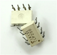
 TLP250光耦合器:资料手册参数分析

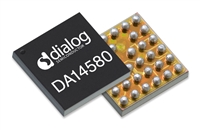
 DA14580 低功耗蓝牙系统级芯片(SoC):资料手册参数分析

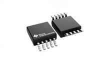
 INA226 高精度电流和功率监控器:资料手册参数分析

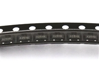
 SI2302 N沟道MOSFET:资料手册参数分析
