Surface Mount
JPS-2-900+
JPS-2-900
Power Splitter/Combiner
2 Way-0° 50Ω
400 to 900 MHz
Maximum Ratings
Features
• low insertion loss, 0.5 dB typ.
• excellent isolation, 24 dB typ.
• excellent VSWR, 1.22:1 typ.
• low amplitude unbalance 0.1 dB typ.
• J-leads for excellent solderability and strain relief
Operating Temperature
Storage Temperature
Power Input (as a splitter)
Internal Dissipation
-40°C to 85°C
CASE STYLE: BH292
-55°C to 100°C
1W max.
+RoHS Compliant
The +Suffix identifies RoHS Compliance. See our web site
for RoHS Compliance methodologies and qualifications
0.125W max.
Permanent damage may occur if any of these limits are
exceeded.
Applications
• cellular
• UHF receivers/transmitters
Pin Connections
SUM PORT
PORT 1
1
3
4
6
Electrical Specifications
PORT 2
GROUND
FREQ.
RANGE
(MHz)
ISOLATION
(dB)
INSERTION LOSS (dB)
ABOVE 3.0 dB
PHASE
UNBALANCE
(Degrees)
AMPLITUDE
UNBALANCE
(dB)
NOT USED
2,5
fL-fU
Typ. Min
Typ. Max.
0.5 1.2
Max.
3.0
Max.
0.4
Outline Drawing
400-900
24
18
PCB Land Pattern
Typical Performance Data
Frequency
(MHz)
Total Loss1
(dB)
Amplitude
Unbalance
(dB)
Isolation
(dB)
Phase
Unbalance
(deg.)
VSWR
S
VSWR
1
VSWR
2
S-1
S-2
400.00
412.50
437.50
462.50
512.50
3.56
3.58
3.50
3.47
3.53
3.57
3.59
3.52
3.46
3.52
0.01
0.01
0.01
0.01
0.01
26.26
26.26
26.14
25.96
25.82
0.74
0.69
0.66
0.69
0.77
1.28
1.28
1.28
1.27
1.27
1.28
1.28
1.27
1.26
1.25
1.30
1.30
1.29
1.28
1.27
Suggested Layout,
Tolerance to be within .002
550.00
587.50
625.00
662.50
700.00
3.53
3.53
3.53
3.59
3.59
3.50
3.48
3.48
3.52
3.51
0.03
0.05
0.05
0.07
0.09
25.67
25.50
25.44
25.41
25.39
0.79
0.84
0.88
1.00
0.97
1.27
1.26
1.25
1.25
1.24
1.24
1.23
1.22
1.22
1.21
1.26
1.25
1.25
1.24
1.23
737.50
775.00
812.50
862.50
900.00
3.56
3.59
3.69
3.66
3.66
3.47
3.49
3.55
3.50
3.48
0.09
0.10
0.13
0.16
0.18
25.43
25.53
25.81
26.05
26.24
1.04
1.05
1.02
1.00
1.11
1.23
1.21
1.20
1.18
1.17
1.20
1.20
1.19
1.18
1.18
1.22
1.21
1.20
1.19
1.19
inch
Outline Dimensions (
)
mm
A
B
C
--
--
D
.100
2.54
E
.225
5.72
F
.055
1.40
G
.280
.310
.100
2.54
7.11
7.87
1. Total Loss = Insertion Loss + 3dB splitter loss.
H
.047
1.19
J
.065
1.65
K
.065
1.65
L
.300
7.62
wt
grams
0.45
JPS-2-900
TOTAL LOSS
JPS-2-900
ISOLATION
40
35
30
25
20
4.0
3.8
3.6
3.4
3.2
3.0
S-1(dB)
S-2(dB)
Demo Board MCL P/N: TB-48+
Suggested PCB Layout (PL-035)
400
500
600
700
800
900
400
500
600
700
800
900
FREQUENCY (MHz)
FREQUENCY (MHz)
JPS-2-900
VSWR
1.5
1.4
1.3
1.2
1.1
1.0
electrical schematic
#S-VSWR
#1-VSWR
#2-VSWR
400
500
600
700
800
900
FREQUENCY (MHz)
Notes
A. Performance and quality attributes and conditions not expressly stated in this specification document are intended to be excluded and do not form a part of this specification document.
B. Electrical specifications and performance data contained in this specification document are based on Mini-Circuit’s applicable established test performance criteria and measurement instructions.
C. The parts covered by this specification document are subject to Mini-Circuits standard limited warranty and terms and conditions (collectively, “Standard Terms”); Purchasers of this part are entitled
to the rights and benefits contained therein. For a full statement of the Standard Terms and the exclusive rights and remedies thereunder, please visit Mini-Circuits’ website at www.minicircuits.com/MCLStore/terms.jsp
REV. D
M151107
JPS-2-900
ED-4852/1
WZ/TD/CP/AM
150817
®
Mini-Circuits
www.minicircuits.com P.O. Box 350166, Brooklyn, NY 11235-0003 (718) 934-4500 sales@minicircuits.com
Page 1 of 1

 5秒后页面跳转


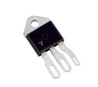 晶闸管的静态特性与伏安特性详解

 贴片电容的工作原理与参数识别
 精密电路设计中的高精电阻:分流电阻
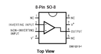 LM7131ACM5手册详解:微型高速单电源运算放大器的深度剖析


 浙公网安备 33010502006866号 浙ICP备10014259号-119
营业执照ICP证
浙公网安备 33010502006866号 浙ICP备10014259号-119
营业执照ICP证


