ICM7242
Absolute Maximum Ratings
Thermal Information
Supply Voltage (V
to V ). . . . . . . . . . . . . . . . . . . . . . . . . . . .18V
SS
Thermal Resistance (Typical, Note2)
θ
(°C/W)
JA
DD
Input Voltage (Note 1)
Terminals (Pins 5, 6, 7, 8). . . . . . . . . . (V -0.3V) to (V
PDIP Package* . . . . . . . . . . . . . . . . . . . . . . . . . . . .
SOIC Package . . . . . . . . . . . . . . . . . . . . . . . . . . . . .
Maximum Storage Temperature Range. . . . . . . . . -65°C to +150°C
Maximum Junction Temperature (Plastic Package) . . . . . . . +150°C
Pb-free reflow profile . . . . . . . . . . . . . . . . . . . . . . . . . .see link below
http://www.intersil.com/pbfree/Pb-FreeReflow.asp
*Pb-free PDIPs can be used for through hole wave solder
processing only. They are not intended for use in Reflow solder
processing applications.
100
160
+0.3V)
DD
SS
Continuous Output Current (Each Output). . . . . . . . . . . . . . . . 50mA
Operating Conditions
Temperature Range
ICM7242I . . . . . . . . . . . . . . . . . . . . . . . . . . . . . . . .-25°C to +85°C
ICM7242C . . . . . . . . . . . . . . . . . . . . . . . . . . . . . . . . 0°C to +70°C
CAUTION: Stresses above those listed in “Absolute Maximum Ratings” may cause permanent damage to the device. This is a stress only rating and operation of the
device at these or any other conditions above those indicated in the operational sections of this specification is not implied.
NOTES:
1. Due to the SCR structure inherent in the CMOS process, connecting any terminal to voltages greater than V
DD
or less than V may cause
SS
destructive device latchup. For this reason, it is recommended that no inputs from external sources not operating on the same supply be applied
to the device before its supply is established and, that in multiple supply systems, the supply to the ICM7242 be turned on first.
2. θ is measured with the component mounted on an evaluation PC board in free air.
JA
Electrical Specifications
PARAMETER
V
= 5V, T = +25°C, R = 10kΩ, C = 0.1µF, V = 0V, Unless Otherwise Specified
DD
A
SS
SYMBOL
TEST CONDITIONS
MIN
TYP
-
MAX
UNITS
V
Guaranteed Supply Voltage
Supply Current
V
2
-
-
-
-
-
-
16
DD
I
Reset
125
340
220
225
5
-
µA
DD
Operating, R = 10kΩ, C = 0.1µF
Operating, R = 1MΩ, C = 0.1µF
TB Inhibited, RC Connected to V
800
µA
600
µA
-
-
-
µA
SS
Timing Accuracy
%
RC Oscillator Frequency Temperature
Drift
Δf/Δt
Independent of RC Components
250
ppm/°C
Time Base Output Voltage
V
I
I
= 100µA
-
-
-
-
-
-
-
-
-
2
-
3.5
0.40
-
-
-
V
V
OTB
SOURCE
= 1.0mA
SINK
Time Base Output Leakage Current
Trigger Input Voltage
I
RC = Ground
25
2.0
4.5
2.0
4.0
-
µA
V
TBLK
V
V
V
V
V
= 5V
1.6
3.5
1.3
2.7
10
1
TRIG
DD
DD
DD
DD
= 15V
= 5V
V
Reset Input Voltage
V
V
RST
= 15V
V
Trigger/Reset Input Current
Max Count Toggle Rate
I
, I
TRIG RST
µA
MHz
MHz
MHz
f
V
V
V
= 2V
= 5V
= 15V
-
T
DD
DD
DD
Counter/Divider Mode
6
-
13
-
50% Duty Cycle Input with Peak to Peak
Voltages Equal to V and V
DD
SS
Output Saturation Voltage
V
All Outputs Except TB Output V
= 5V,
-
0.22
0.4
V
SAT
DD
I
= 3.2mA
OUT
Output Sourcing Current
I
V
= 5V Terminals 2 and 3, V
= 1V
-
300
-
-
µA
pF
Ω
SOURCE
DD
OUT
MIN Timing Capacitor (Note 3)
Timing Resistor Range (Note 3)
C
10
1k
-
-
T
T
R
V
= 2 - 16V
22M
DD
NOTE:
3. For design only, not tested.
FN2866.4
February 9, 2007
3


 SI2301 N沟道MOSFET:资料手册参数分析

 ADC0809逐次逼近寄存器型模数转换器:资料手册参数分析

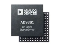
 AD9361捷变收发器:全面参数解析与关键特性概览

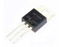
 IRF3205功率MOSFET:资料手册参数分析
