Symbol
Type
Function
Auto-precharge: A10 is sampled during Read/Write commands to determine whether
Autoprecharge should be performed to the accessed bank after the Read/Write
operation. (HIGH: Autoprecharge; LOW: no Autoprecharge). A10 is sampled during a
Precharge command to determine whether the Precharge applies to one bank (A10
LOW) or all banks (A10 HIGH). If only one bank is to be precharged, the bank is
selected by bank addresses.
A10 / AP
Input
Burst Chop: A12 / BC_n is sampled during Read and Write commands to determine if
A12 / BC_n
RESET_n
Input burst chop (on-the-fly) will be performed. (HIGH, no burst chop; LOW: burst chopped).
See command truth table for details.
CMOS Active Low Asynchronous Reset: Reset is active when RESET_n is LOW, and inactive
Input when RESET_n is HIGH. RESET_n must be HIGH during normal operation.
Data Input/ Output: Bi-directional data bus. If CRC is enabled via Mode register, then
Input / CRC code is added at the end of Data Burst. Any DQ from DQ0-DQ3 may indicate the
Output internal Vref level during test via Mode Register Setting MR4 A4=High. Refer to vendor
specific data sheets to determine which DQ is used.
DQ
Dummy load for matching the loading for mixed populations of x8 based RDIMMs and
x4 based RDIMMs. Not used on LRDIMMs.
TDQS9_t-TDQS17_t
TDQS9_c-TDQS17_c
Input
Input/ Data Bus Inversion. Not used on LRDIMMs.
Output
DBI0_n-DBI8_n
DM0_n-DM8_n
Input
Data Mask. Not used on LRDIMMs.
Data Strobe: output with read data, input with write data. Edge-aligned with read data,
DQS0_t-DQS17_t, Input / centered in write data. The data strobe DQS_t is paired with differential signals DQS_c,
DQS0_c-DQS17_c Output respectively, to provide differential pair signaling to the system during reads and writes.
DDR4 SDRAM supports differential data strobe only and does not support single-ended.
Command and Address Parity Input : DDR4 Supports Even Parity check in DRAMs with
MR setting. Once it’s enabled via Register in MR5, then DRAM calculates Parity with
PAR
Input ACT_n, RAS_n/A16, CAS_n/A15, WE_n/A14, BG0-BG1, BA0-BA1, A17-A0. Input parity
should be maintained at the rising edge of the clock and at the same time with
command & address with CS_n LOW.
Alert: It has multi functions such as CRC error flag, Command and Address Parity error
flag as Output signal. If there is an error in the CRC, then ALERT_n goes LOW for the
Output period time interval and goes back HIGH. If there is an error in the Command Address
(Input) Parity Check, then ALERT_n goes LOW for a relatively long period until the on going
DRAM internal recovery transaction is complete. During Connectivity Test mode, this
pin functions as an input. Whether ALERT_n is used or not is system dependent.
ALERT_n
RFU
NC
Reserved for Future Use: No on-DIMM electrical connection is present.
No Connect: No internal electrical connection is present.
VDD
VSS
VTT
VPP
Supply
Supply
Supply
Supply
Power Supply: 1.2 V ± 0.06 V
Ground
Power Supply for termination of Address, Command and Control, VDD/2.
DRAM Activating Power Supply: 2.5V (2.375V min , 2.75V max)
Rev. 1.0 / Nov.2020
7


 深入解析AD7606高性能多通道模数转换器:资料手册参数分析

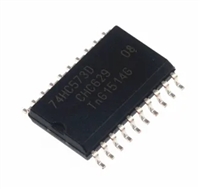
 74HC573三态非易失锁存器(Latch)资料手册参数分析

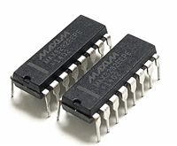
 MAX3232 RS-232电平转换器资料手册参数分析

 MAX485 RS-485/RS-422收发器资料手册参数分析
